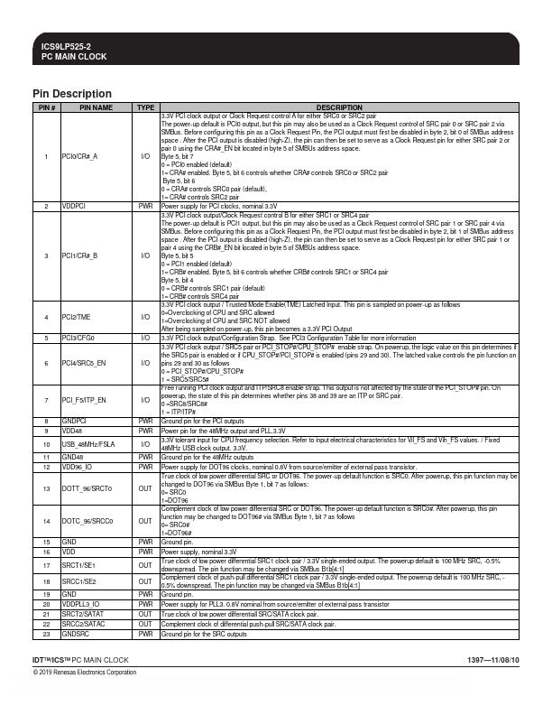
Description
PIN #
PIN NAME
1 PCI0/CR#_A
2 VDDPCI
3 PCI1/CR#_B
4 PCI2/TME
5 PCI3/CFG0
6 PCI4/SRC5_EN
7 PCI_F5/ITP_EN
8 GNDPCI 9 VDD48 10 USB_48MHz/FSLA 11 GND48 12 VDD96_IO
13 DOTT_96/SRCT0
14 DOTC_96/SRCC0
15 GND 16 VDD 17 SRCT1/SE1 18 SRCC1/SE2 19 GND 20 VDDPLL3_IO 21 SRCT2/SATAT 22 SRCC2/SATAC 23 GNDSRC
TYPE
I/O
PWR
I/O
I/O I/O I/O
I/O PWR PWR I/O PWR PWR OUT
OUT PWR PWR OUT OUT PWR PWR OUT OUT PWR
DESCRIPTION 3.3V PCI clock output or Clock Request control A for either SRC0 or SRC2 pair The power-
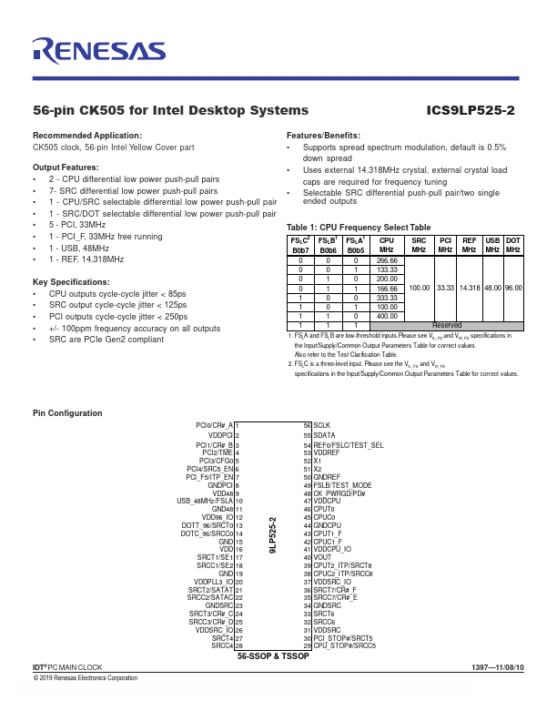
Features
- 2 - CPU differential low power push-pull pairs.
- 7- SRC differential low power push-pull pairs.
- 1 - CPU/SRC selectable differential low power push-pull pair.
- 1 - SRC/DOT selectable differential low power push-pull pair.
- 5 - PCI, 33MHz.
- 1 - PCI_F, 33MHz free running.
- 1 - USB, 48MHz.
- 1 - REF, 14.318MHz
Key Specifications:.
- CPU outputs cycle-cycle jitter < 85ps.
- SRC output cycle-cycle jitter < 125ps.
 9LP525-2-Renesas.pdf