Datasheet Details
| Part number | CD4015BMS |
|---|---|
| Manufacturer | Intersil Corporation |
| File Size | 118.73 KB |
| Description | CMOS Dual 4-Stage Static Shift Register |
| Datasheet |
 CD4015BMS_IntersilCorporation.pdf CD4015BMS_IntersilCorporation.pdf
|
| Part number | CD4015BMS |
|---|---|
| Manufacturer | Intersil Corporation |
| File Size | 118.73 KB |
| Description | CMOS Dual 4-Stage Static Shift Register |
| Datasheet |
CD4015BMS_IntersilCorporation.pdf
|
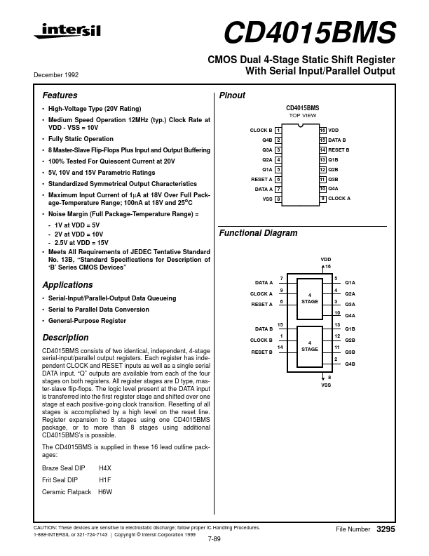
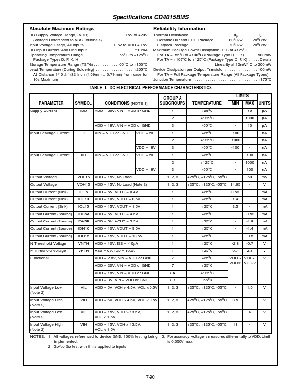
of ‘B’ Series CMOS Devices” Functional Diagram VDD 16 DATA A CLOCK A RESET A 7 9 6 4 STAGE 5 4 3 10 DATA B 15 1 14 RESET B 4 STAGE 13 12 Q2B 11 Q3B 2 Q4B 8 VSS Q1A Q2A Q3A Q4A Q1B Applications Serial-Input/Parallel-Output Data Queueing Serial to Parallel Data Conversion General-Purpose Register Description CD4015BMS consists of two identical, independent, 4-stage serial-input/parallel output registers.Each register has independent CLOCK and RESET inputs as well
📁 CD4015BMS Similar Datasheet