Datasheet Details
- Part number
- HI3197
- Manufacturer
- Intersil Corporation
- File Size
- 336.47 KB
- Datasheet
- HI3197_IntersilCorporation.pdf
- Description
- 125 MSPS D/A Converter
HI3197 Description
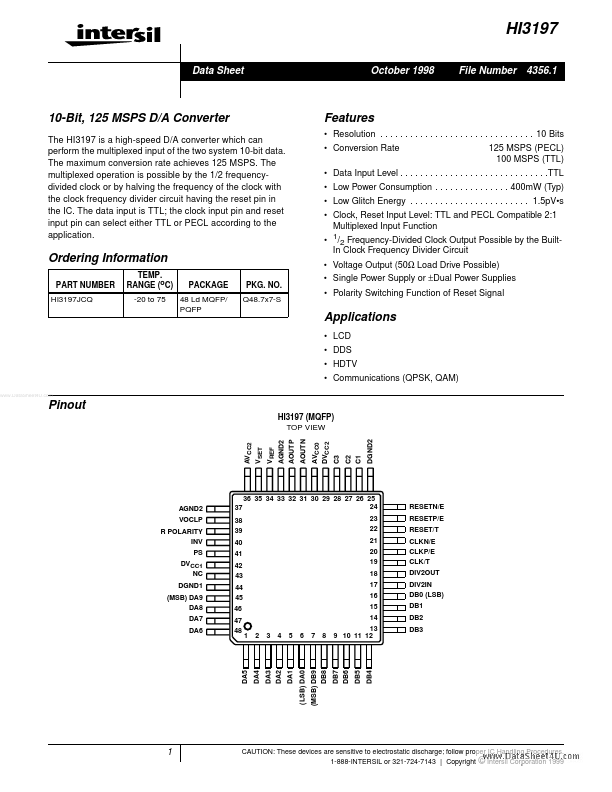
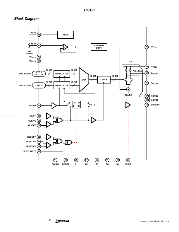
HI3197 Data Sheet October 1998 File Number 4356.1 10-Bit, 125 MSPS D/A Converter The HI3197 is a high-speed D/A converter which can perform the multi.
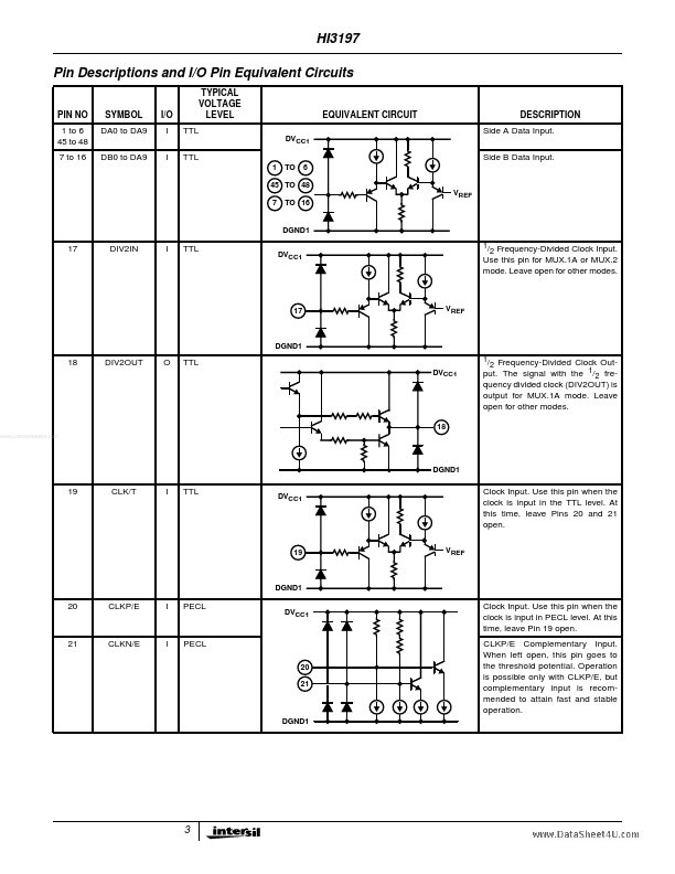
and I/O Pin Equivalent Circuits
PIN NO 1 to 6 45 to 48 7 to 16 SYMBOL DA0 to DA9 DB0 to DA9 I/O I I TYPICAL VOLTAGE LEVEL TTL
DVCC1
EQUIVALENT CIRCU.
HI3197 Features
* Resolution
* . 10 Bits
* Conversion Rate 125 MSPS (PECL) 100 MSPS (TTL)
* Data Input Level
* . . . . . TTL
* Low Power Consumption
* 400mW (Typ)
HI3197 Applications
* LCD
* DDS
* HDTV
* Communications (QPSK, QAM)
www. DataSheet4U. com
Pinout
HI3197 (MQFP) TOP VIEW
AOUTN AGND2 AOUTP AVCC2 DGND2 AVCC0 DVCC2 VREF VSET
AGND2 VOCLP R POLARITY INV PS DVCC1 NC DGND1 (MSB) DA9 DA8 DA7 DA6
37 38 39 40 41 42 43 44 45 46 47 48
36 35 34 3
📁 Related Datasheet
📌 All Tags
HI3197 Stock/Price