Datasheet Details
| Part number | PL133-27 |
|---|---|
| Manufacturer | Micrel |
| File Size | 236.19 KB |
| Description | 1:2 Fanout Buffer IC |
| Datasheet |
 PL133-27 Datasheet PL133-27 Datasheet
|
|
|
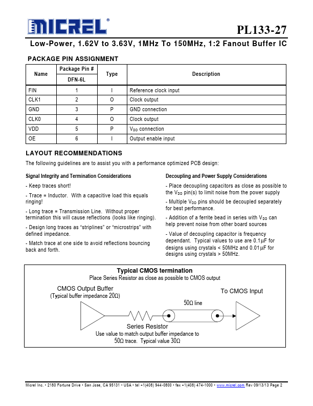
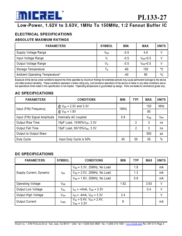
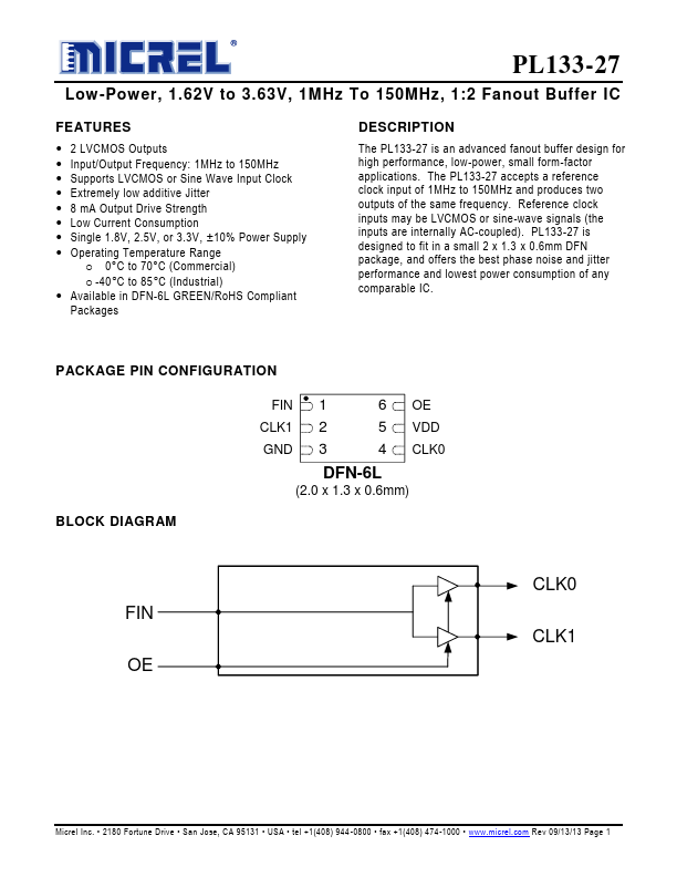
The PL133-27 is an advanced fanout buffer design for high performance, low-power, small form-factor applications.
The PL133-27 accepts a reference clock input of 1MHz to 150MHz and produces two outputs of the same frequency.
| Part number | PL133-27 |
|---|---|
| Manufacturer | Micrel |
| File Size | 236.19 KB |
| Description | 1:2 Fanout Buffer IC |
| Datasheet |
PL133-27 Datasheet
|
|
|
|