Description
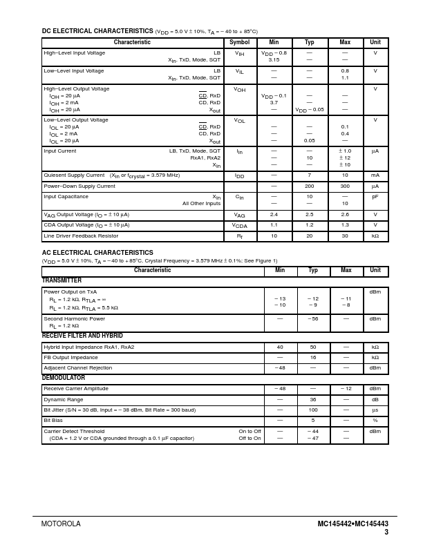
ABSOLUTE MAXIMUM RATINGS (Voltages Referenced to VSS)
Rating Supply Voltage DC Input Voltage DC Output Voltage Clamp Diode Current, per Pin DC Output Current, per Pin Power Dissipation Operating Temperature Range Storage Temperature Range Symbol VDD Vin Vout IIK, IOK Iout PD TA Tstg Value
0.5 to + 7.0
0.5 to VDD + 0.5
0.5 to VDD + 0.5 ± 20 ± 28 500
40 to + 85
65 to + 150 Unit V V V mA mA mW °C °C This device contains circuitry to protect the in
Features
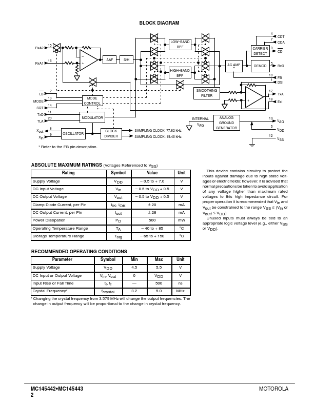
- d. ) When LB is connected to analog ground (VAG), the modulator generates an echo cancellation tone of 2100 Hz for MC145442 CCITT V.21 and 2225 Hz for MC145443 Bell 103 systems. For normal operation, this pin should be at a logic low level (VSS). The power.
- down mode is enabled when both LB and SQT are connected to a logic high level (see Table 2). Table 2. Functional Table
MODE Pin 13 1 0 X X X X X SQT Pin 14 0 0 0 0 1 1 1 LB Pin 2 0 0 VAG (VDD/2) 1 0 VAG (VDD/2) 1 Operating Mode Originat.
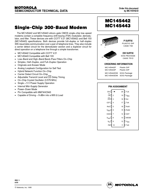
 MC145442_Motorola.pdf