Description
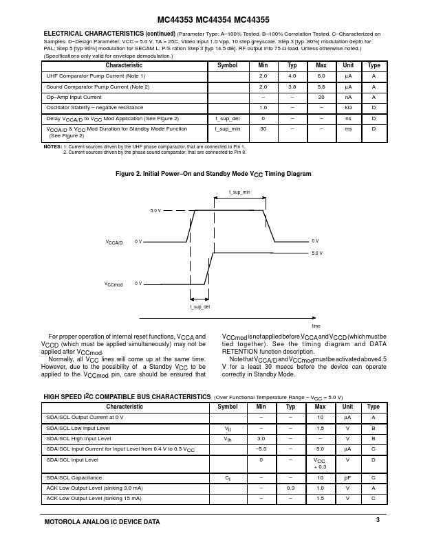
Note that VCCA/D and VCCmod must be activated above 4.5 V for a least 30 msecs before the device can operate correctly in Standby Mode.
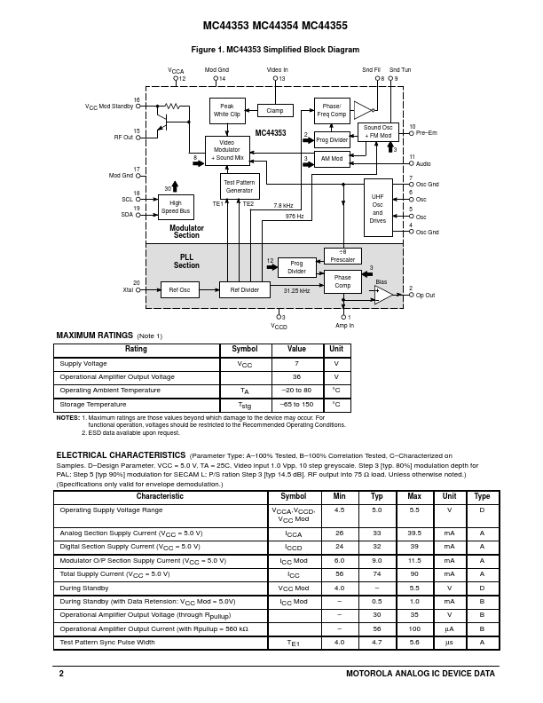
VCC = 5.0 V)
Characteristic SDA/SCL Output Current at 0 V SDA/SCL Low Input Level SDA/SCL High Input Level SDA/SCL Input Current for Input Level from 0.4 V to 0.3 VCC SDA/SCL Input Level SDA/SCL Capacitance ACK Low Output Level (sinking 3.0 mA) ACK Low Output Level (sink
Features
- 355 PSD0.
- 1 are Don’t Care). 7. SysL: System L enable (selects AM sound and positive video modulation, MC44353 only). 8. TPEN: Test pattern enable (picture and sound). 9. N0 to N11: UHF frequency programming bits, in steps of 250 kHz. Figure 5. High Speed I2C Compatible bus data format
SCL 1 2 3 4 5 6 7 8 9 10 11 12 13 14 15 16 17 18 19 44 45
STA SDA
Chip Address ($CA) ACK
First Data Byte (C1 or FM) ACK
Data ACK
STO.
 MC44353-Motorola.pdf