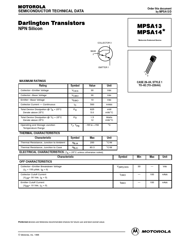
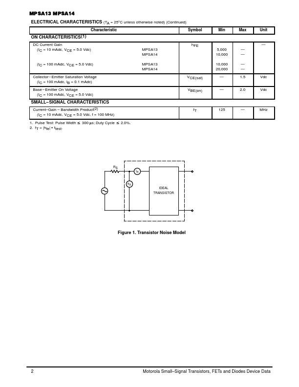
MPSA13 Overview
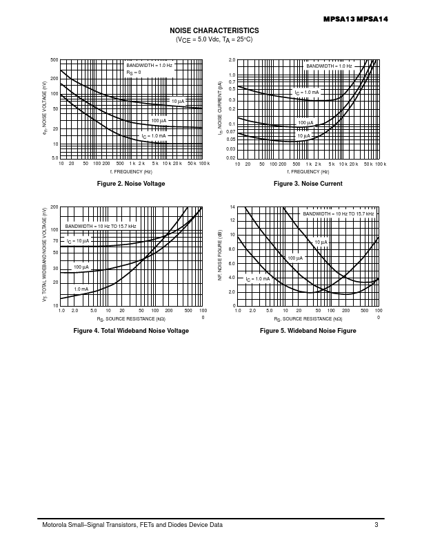
Motorola Small Signal Transistors, FETs and Diodes Device Data © Motorola, Inc. RS in en IDEAL TRANSISTOR Figure 1. Total Wideband Noise Voltage Figure.
MPSA13 datasheet by Motorola Semiconductor (now NXP Semiconductors).
| Part number | MPSA13 |
|---|---|
| Datasheet | MPSA13_Motorola.pdf |
| File Size | 225.92 KB |
| Manufacturer | Motorola Semiconductor (now NXP Semiconductors) |
| Description | Darlington Transistors |
|
|
Motorola Small Signal Transistors, FETs and Diodes Device Data © Motorola, Inc. RS in en IDEAL TRANSISTOR Figure 1. Total Wideband Noise Voltage Figure.
| Brand Logo | Part Number | Description | Other Manufacturers |
|---|---|---|---|
| MPSA13 | NPN Darlington Transistor | Fairchild Semiconductor | |
| MPSA13 | EPITAXIAL PLANAR NPN TRANSISTOR | KEC | |
| MPSA13 | NPN Silicon Darlington Transistor | MCC | |
| MPSA13 | Plastic-Encapsulate Transistros NPN Darlington Transistor | Weitron Technology | |
| MPSA13 | NPN Silicon Transistor | ON Semiconductor |
View all Motorola Semiconductor (now NXP Semiconductors) datasheets
| Part Number | Description |
|---|---|
| MPSA12 | DARLINGTON TRANSISTOR |
| MPSA14 | Darlington Transistors |
| MPSA16 | (MPSA17) Chopper Transistors |
| MPSA17 | NPN Chopper Transistor |
| MPSA18 | Low Noise Transistor |
| MPSA05 | Amplifier Transistors |
| MPSA06 | Amplifier Transistors |
| MPSA20 | Amplifier Transistor(NPN Silicon) |
| MPSA25 | DARLINGTON TRANSISTOR |
| MPSA26 | DARLINGTON TRANSISTOR |