Datasheet Details
| Part number | NX3L1G66 |
|---|---|
| Manufacturer | NXP Semiconductors |
| File Size | 168.45 KB |
| Description | Low-voltage analog switch |
| Datasheet |
 NX3L1G66 Datasheet NX3L1G66 Datasheet
|
|
|
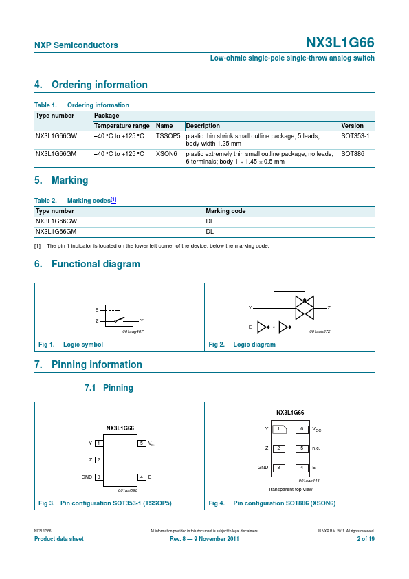
The NX3L1G66 is a low-ohmic single-pole single-throw analog switch.
It has two input/output terminals (Y and Z) and an active HIGH enable input pin (E).
When E is LOW, the analog switch is turned off.
| Part number | NX3L1G66 |
|---|---|
| Manufacturer | NXP Semiconductors |
| File Size | 168.45 KB |
| Description | Low-voltage analog switch |
| Datasheet |
NX3L1G66 Datasheet
|
|
|
|