Datasheet Details
- Part number
- 74ABT5074
- Manufacturer
- NXP ↗
- File Size
- 100.92 KB
- Datasheet
- 74ABT5074_PhilipsSemiconductors.pdf
- Description
- Synchronizing dual D-type flip-flop
74ABT5074 Description
Philips Semiconductors Advanced BiCMOS Products Product specification Synchronizing dual D-type flip-flop with metastable immune characteristics 74.
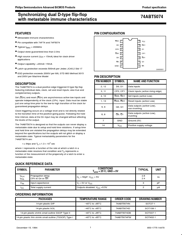
PIN NUMBER 2, 12 3, 11 4, 10 1, 13 5, 9 6, 8 7 14 SYMBOL D0, D1 CP0, CP1 SD0, SD1 RD0, RD1 Q0, Q1 Q0, Q1 GND VCC NAME AND FUNCTION Data inputs Clock i.
74ABT5074 Features
* Metastable immune characteristics
* Pin compatible with 74F74 and 74F5074
* Typical fMAX = 200MHz
* Output skew guaranteed less than 2.0ns
74ABT5074 Applications
* PIN CONFIGURATION
RD0 D0 CP0 SD0 Q0 Q0 GND 1 2 3 4 5 6 7 14 13 12 11 10 9 8 VCC RD1 D1 CP1 SD1 Q1 Q1
* Output capability: +20mA/
* 15mA
* Latch-up protection exceeds 500mA per Jedec JC40.2 Std 17
* ESD protection exceeds 2000V per MIL STD 883 Method 3015
and 200V per
📁 Related Datasheet
📌 All Tags