Datasheet Details
| Part number | 74LVC241A |
|---|---|
| Manufacturer | NXP |
| File Size | 181.81 KB |
| Description | Octal buffer/line driver |
| Datasheet |
 74LVC241A Datasheet 74LVC241A Datasheet
|
|
|
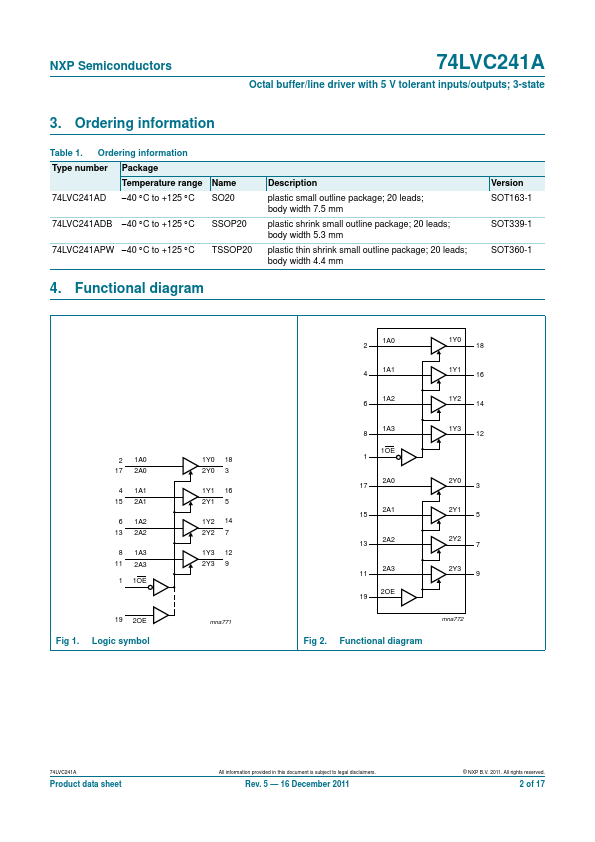
The 74LVC241A is an octal non-inverting buffer/line driver with 3-state outputs.
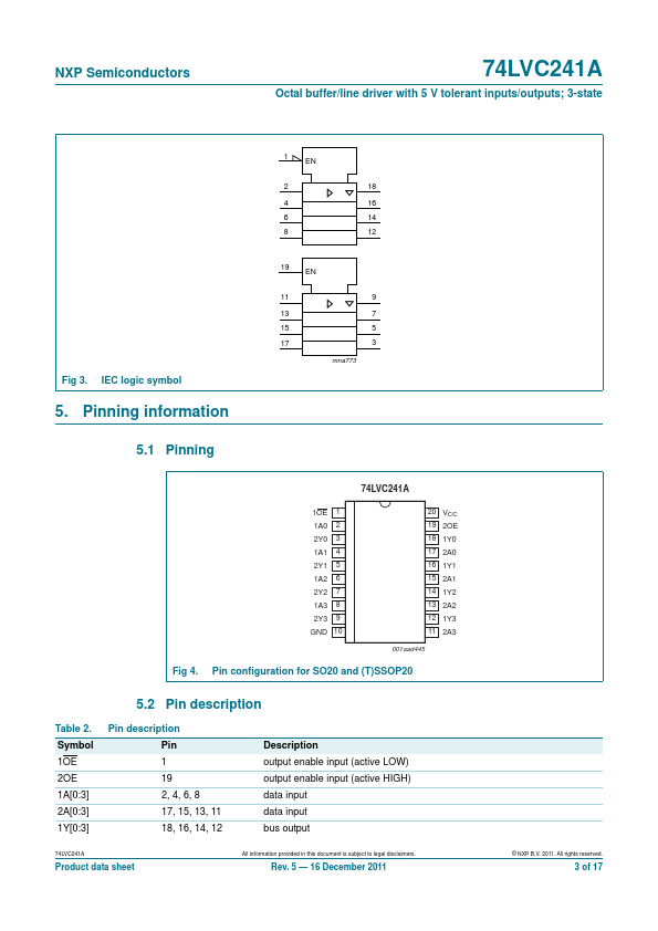
The 3-state outputs are controlled by the output enable inputs (pins 1OE and 2OE).
Schmitt trigger action at all inputs makes the circuit highly tolerant of slower input rise and fall times.
| Part number | 74LVC241A |
|---|---|
| Manufacturer | NXP |
| File Size | 181.81 KB |
| Description | Octal buffer/line driver |
| Datasheet |
74LVC241A Datasheet
|
|
|
|