These hex buffers are monolithic complementary MOS (CMOS) integrated circuits constructed with N- and P-channel enhancement mode transistors These devices feature logic level conversion using only one supply voltage (VDD) The input signal high level (VIH) can exceed the VDD supply voltage when these
Features
Y Y
Y Y
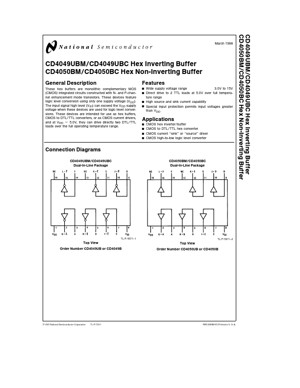
Wide supply voltage range 3 0V to 15V Direct drive to 2 TTL loads at 5 0V over full temperature range High source and sink current capability Special input protection permits input voltages greater than VDD.
CD4051BC- Single 8-Channel/ Dual 4-Channel/ Triple 2-Channel Analog Multiplexer/Demultiplexe
CD4051BM- Single 8-Channel/ Dual 4-Channel/ Triple 2-Channel Analog Multiplexer/Demultiplexe
CD4051C- Single 8-Channel Analog Multiplexer/Demultiplexer
CD4051M- Single 8-Channel Analog Multiplexer/Demultiplexer
CD4052BC- Single 8-Channel/ Dual 4-Channel/ Triple 2-Channel Analog Multiplexer/Demultiplexe
CD4052BM- Single 8-Channel/ Dual 4-Channel/ Triple 2-Channel Analog Multiplexer/Demultiplexe
CD4052C- Dual 4-Channel Analog Multiplexer/Demultiplexer
Full PDF Text Transcription
Click to expand full text
CD4049UBM CD4049UBC Hex Inverting Buffer CD4050BM CD4050BC Hex Non-Inverting Buffer
March 1988
CD4049UBM CD4049UBC Hex Inverting Buffer CD4050BM CD4050BC Hex Non-Inverting Buffer
General Description
These hex buffers are monolithic complementary MOS (CMOS) integrated circuits constructed with N- and P-channel enhancement mode transistors These devices feature logic level conversion using only one supply voltage (VDD) The input signal high level (VIH) can exceed the VDD supply voltage when these devices are used for logic level conversions These devices are intended for use as hex buffers CMOS to DTL TTL converters or as CMOS current drivers and at VDD e 5 0V they can drive directly two DTL TTL loads over the full operating temperature range
Features
Y Y
Y Y
Wide supply voltage range 3
 CD4050BC Datasheet