Click to expand full text
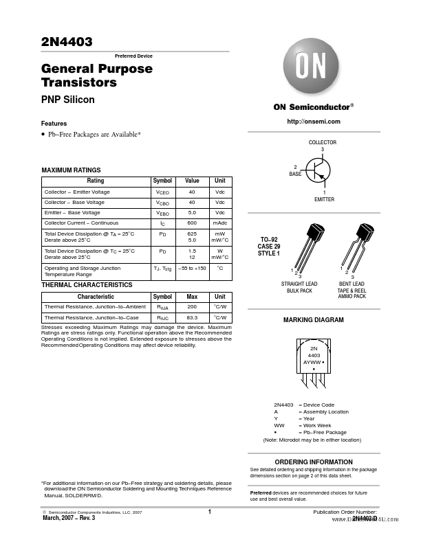
2N4403
Preferred Device
General Purpose Transistors
PNP Silicon
Features
• Pb−Free Packages are Available*
MAXIMUM RATINGS
Rating
Symbol Value
Unit
Collector − Emitter Voltage Collector − Base Voltage Emitter − Base Voltage Collector Current − Continuous Total Device Dissipation @ TA = 25°C Derate above 25°C
VCEO VCBO VEBO
IC PD
40
Vdc
40
Vdc
5.0
Vdc
600
mAdc
625
mW
5.0
mW/°C
Total Device Dissipation @ TC = 25°C Derate above 25°C
PD
1.5
W
12
mW/°C
Operating and Storage Junction Temperature Range
TJ, Tstg −55 to +150 °C
THERMAL CHARACTERISTICS
Characteristic
Symbol
Max
Unit
Thermal Resistance, Junction−to−Ambient RqJA
200
°C/W
Thermal Resistance, Junction−to−Case
RqJC
83.3
°C/W
Stresses exceeding Maximum Ratings may damage the device.
 2N4403G Datasheet