FDC6327C Overview
Key Specifications
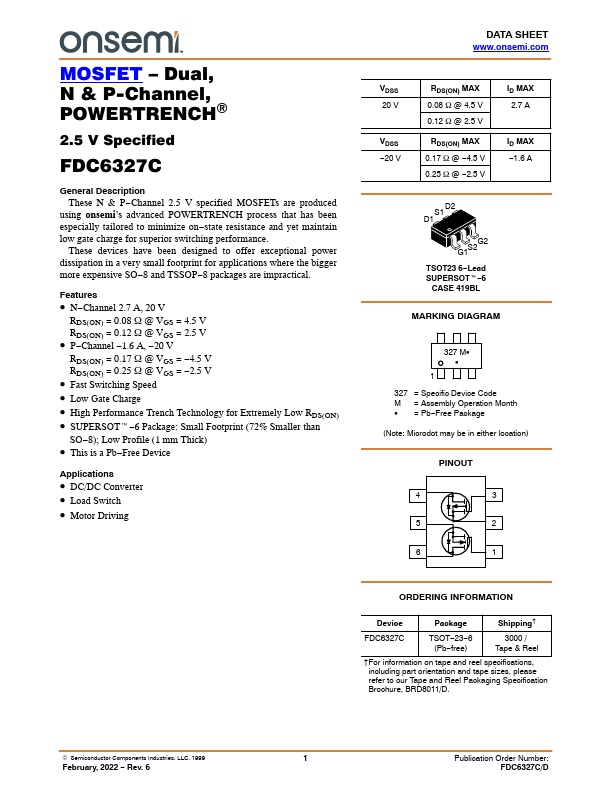
Package: SOT-23-6
Mount Type: Surface Mount
Pins: 6
Height: 1.1 mm
Description
These N & P-Channel 2.5 V specified MOSFETs are produced using onsemi’s advanced POWERTRENCH process that has been especially tailored to minimize on-state resistance and yet maintain low gate charge for superior switching performance. These devices have been designed to offer exceptional power dissipation in a very small footprint for applications where the bigger more expensive SO-8 and TSSOP-8 packages are impractical.
Key Features
- N-Channel 2.7 A, 20 V RDS(ON) = 0.08 W @ VGS = 4.5 V RDS(ON) = 0.12 W @ VGS = 2.5 V
- P-Channel -1.6 A, -20 V RDS(ON) = 0.17 W @ VGS = -4.5 V RDS(ON) = 0.25 W @ VGS = -2.5 V
- Fast Switching Speed
- Low Gate Charge
- High Performance Trench Technology for Extremely Low RDS(ON)