Click to expand full text
www.DataSheet4U.com
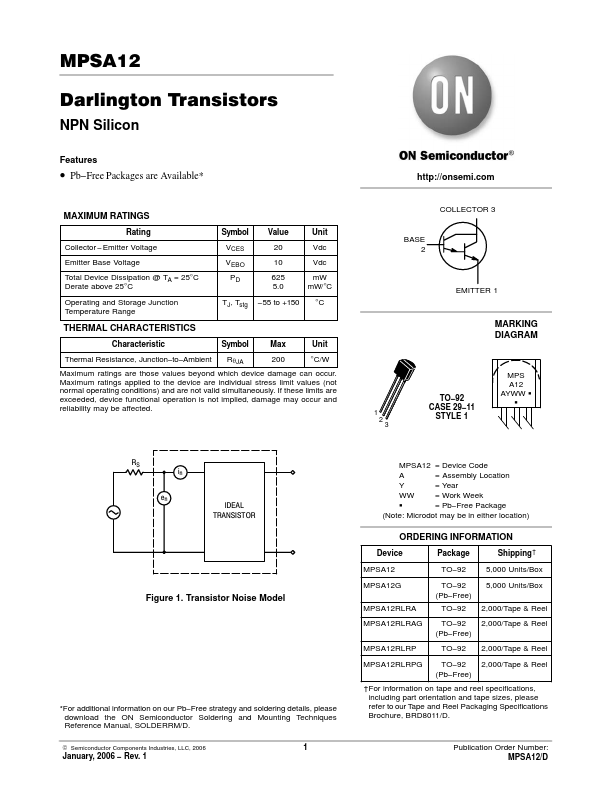
MPSA12 Darlington Transistors
NPN Silicon
Features
• Pb−Free Packages are Available*
MAXIMUM RATINGS
Rating Collector −Emitter Voltage Emitter Base Voltage Total Device Dissipation @ TA = 25°C Derate above 25°C Operating and Storage Junction Temperature Range Symbol VCES VEBO PD TJ, Tstg Value 20 10 625 5.0 −55 to +150 Unit Vdc Vdc mW mW/°C °C
http://onsemi.com
COLLECTOR 3
BASE 2
EMITTER 1
THERMAL CHARACTERISTICS
Characteristic Thermal Resistance, Junction−to−Ambient Symbol RqJA Max 200 Unit °C/W
MARKING DIAGRAM
Maximum ratings are those values beyond which device damage can occur. Maximum ratings applied to the device are individual stress limit values (not normal operating conditions) and are not valid simultaneously.
 MPSA12 Datasheet