Datasheet Details
| Part number | NB3N51032 |
|---|---|
| Manufacturer | ON Semiconductor ↗ |
| File Size | 435.73 KB |
| Description | Dual HCSL/LVDS Clock Generator |
| Datasheet |
 NB3N51032-ONSemiconductor.pdf NB3N51032-ONSemiconductor.pdf
|
| Part number | NB3N51032 |
|---|---|
| Manufacturer | ON Semiconductor ↗ |
| File Size | 435.73 KB |
| Description | Dual HCSL/LVDS Clock Generator |
| Datasheet |
NB3N51032-ONSemiconductor.pdf
|
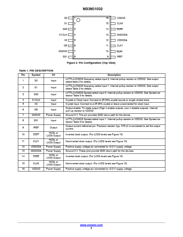
Pin Symbol I/O 1 S0 Input 2 S1 Input 3 SS0 Input 4 X1/CLK 5 X2 Input Input 6 OE Input 7 GNDXD Power Supply 8 SS1 Input 9 IREF Output 10 CLK1 HCSL or LVDS Output 11 CLK1 HCSL or LVDS Output 12 VDDODA Power Supply 13 GNDODA Power Supply 14 CLK0 HCSL or LVDS Output 15 CLK0 HCSL or LVDS Output 16 VDDXD Power Supply Description LVTTL/LVCMOS frequency select input 0. Internal pullup resistor to VDDXD.See output select table 2 for details.LVTTL/LVCMOS fr
📁 NB3N51032 Similar Datasheet