Datasheet Details
| Part number | NB3N51034 |
|---|---|
| Manufacturer | ON Semiconductor ↗ |
| File Size | 434.55 KB |
| Description | Quad HCSL - LVDS Clock Generator |
| Datasheet |
 NB3N51034-ONSemiconductor.pdf NB3N51034-ONSemiconductor.pdf
|
| Part number | NB3N51034 |
|---|---|
| Manufacturer | ON Semiconductor ↗ |
| File Size | 434.55 KB |
| Description | Quad HCSL - LVDS Clock Generator |
| Datasheet |
NB3N51034-ONSemiconductor.pdf
|
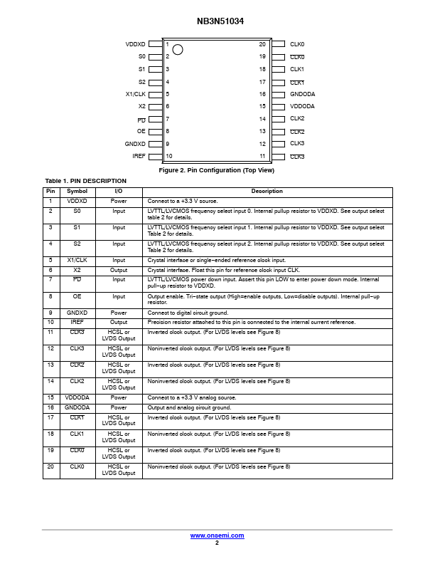
Pin Symbol I/O 1 VDDXD Power 2 S0 Input 3 S1 Input 4 S2 Input 5 X1/CLK 6 X2 7 PD Input Output Input 8 OE Input 9 GNDXD 10 IREF 11 CLK3 12 CLK3 13 CLK2 14 CLK2 15 VDDODA 16 GNDODA 17 CLK1 18 CLK1 19 CLK0 20 CLK0 Power Output HCSL or LVDS Output HCSL or LVDS Output HCSL or LVDS Output HCSL or LVDS Output Power Power HCSL or LVDS Output HCSL or LVDS Output HCSL or LVDS Output HCSL or LVDS Output Figure 2. Pin Configuration (Top View) Description Connect to a +3.3 V source.LVTTL/LV
📁 NB3N51034 Similar Datasheet