Datasheet Details
| Part number | NB3N51044 |
|---|---|
| Manufacturer | ON Semiconductor ↗ |
| File Size | 130.89 KB |
| Description | Quad HCSL / LVDS Clock Generator |
| Datasheet |
 NB3N51044-ONSemiconductor.pdf NB3N51044-ONSemiconductor.pdf
|
| Part number | NB3N51044 |
|---|---|
| Manufacturer | ON Semiconductor ↗ |
| File Size | 130.89 KB |
| Description | Quad HCSL / LVDS Clock Generator |
| Datasheet |
NB3N51044-ONSemiconductor.pdf
|
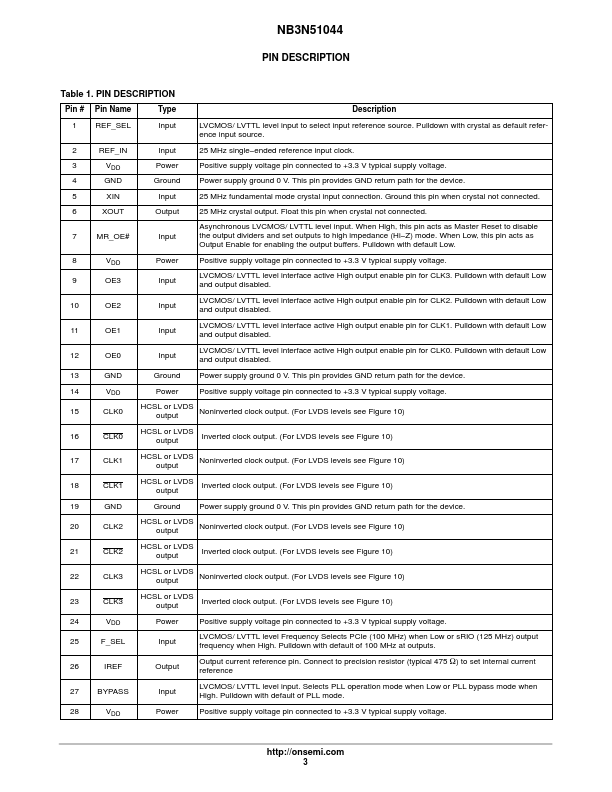
Table 1.
📁 NB3N51044 Similar Datasheet