Datasheet Details
| Part number | NB3N51054 |
|---|---|
| Manufacturer | ON Semiconductor ↗ |
| File Size | 162.85 KB |
| Description | Quad HCSL / LVDS Clock Generator |
| Datasheet |
 NB3N51054-ONSemiconductor.pdf NB3N51054-ONSemiconductor.pdf
|
| Part number | NB3N51054 |
|---|---|
| Manufacturer | ON Semiconductor ↗ |
| File Size | 162.85 KB |
| Description | Quad HCSL / LVDS Clock Generator |
| Datasheet |
NB3N51054-ONSemiconductor.pdf
|
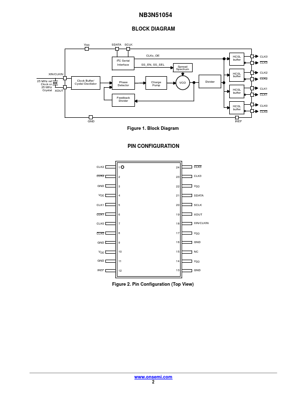
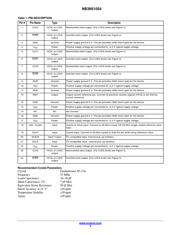
Pin # Pin Name Type 1 CLK2 HCSL or LVDS output Description Noninverted clock output.(For LVDS levels see Figure 4) 2 CLK2 HCSL or LVDS Inverted clock output.(For LVDS levels see Figure 4) output 3 GND Ground Power supply ground 0 V.This pin provides GND return path for the device.4 VDD Power Positive supply voltage pin connected to +3.3 V typical supply voltage.5 CLK1 HCSL or LVDS Noninverted clock output.(For LVDS levels see Figure 4) output 6 CLK1 HCSL or LVDS Inv
📁 NB3N51054 Similar Datasheet