Datasheet Details
| Part number | NB3N853501E |
|---|---|
| Manufacturer | ON Semiconductor |
| File Size | 208.54 KB |
| Description | 3.3V LVTTL/LVCMOS 2:1 MUX to 4 LVPECL Differential Clock Fanout Buffer Outputs |
| Datasheet |
 NB3N853501E Datasheet NB3N853501E Datasheet
|
|
|
| Part number | NB3N853501E |
|---|---|
| Manufacturer | ON Semiconductor |
| File Size | 208.54 KB |
| Description | 3.3V LVTTL/LVCMOS 2:1 MUX to 4 LVPECL Differential Clock Fanout Buffer Outputs |
| Datasheet |
NB3N853501E Datasheet
|
|
|
|
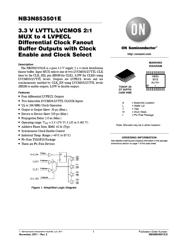
The NB3N853501E is a pure 3.3 V supply 2:1:4 clock distribution fanout buffer.Input MUX selects one of two LVCMOS/LVTTL CLK lines by the CLK_SEL pin (HIGH for CLK1, LOW for CLK0) using LVCMOS/LVTTL levels.Outputs are LVPECL levels and are synchronously enabled by CLK_EN using LVCMOS/LVTTL levels (HIGH to enable outputs, LOW to disable output).
📁 Similar Datasheet