Datasheet Details
- Part number
- NB4N11M
- Manufacturer
- ON Semiconductor ↗
- File Size
- 273.37 KB
- Datasheet
- NB4N11M_ONSemiconductor.pdf
- Description
- Multi Level Clock/Data Input to CML Receiver/Buffer/Translator
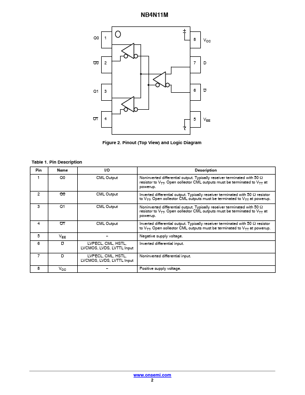
NB4N11M Description
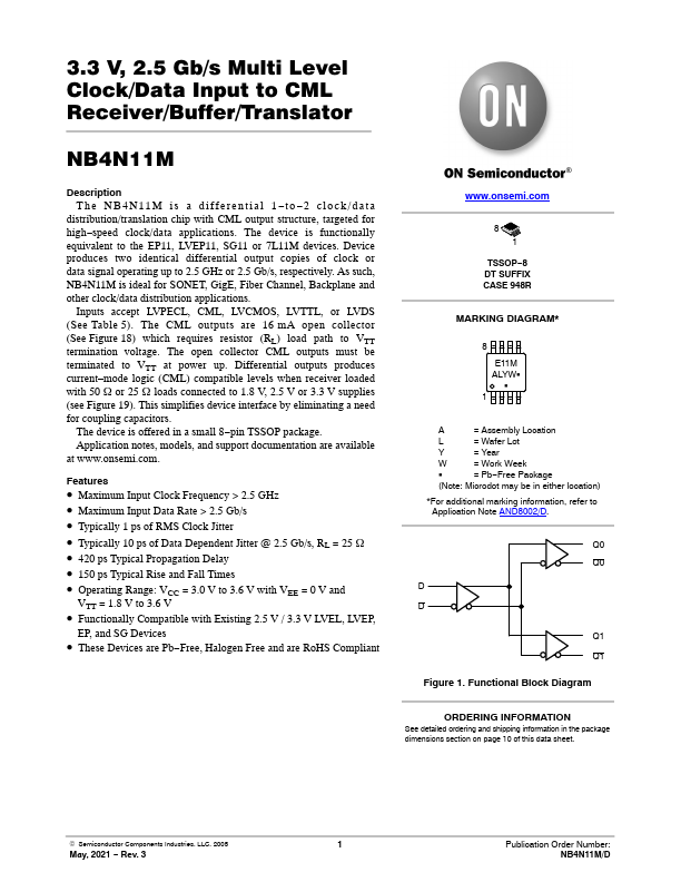
3.3 V, 2.5 Gb/s Multi Level Clock/Data Input to CML Receiver/Buffer/Translator NB4N11M .
The NB4N11M is a differential 1.
to.
2 clock/data
distribution/translation chip with CML output structure, targeted for high.
spe.
NB4N11M Features
* Maximum Input Clock Frequency > 2.5 GHz
* Maximum Input Data Rate > 2.5 Gb/s
* Typically 1 ps of RMS Clock Jitter
* Typically 10 ps of Data Dependent Jitter @ 2.5 Gb/s, RL = 25 W
* 420 ps Typical Propagation Delay
* 150 ps Typical Rise and Fall Times
NB4N11M Applications
* The device is functionally equivalent to the EP11, LVEP11, SG11 or 7L11M devices. Device produces two identical differential output copies of clock or data signal operating up to 2.5 GHz or 2.5 Gb/s, respectively. As such, NB4N11M is ideal for SONET, GigE, Fiber Channel, Backplane and other clock/d
📁 Related Datasheet
📌 All Tags