Datasheet Details
- Part number
- NB4N11S
- Manufacturer
- ON Semiconductor ↗
- File Size
- 131.38 KB
- Datasheet
- NB4N11S_ONSemiconductor.pdf
- Description
- 3.3V 1:2 AnyLevel Input to LVDS Fanout Buffer /Translator
NB4N11S Description
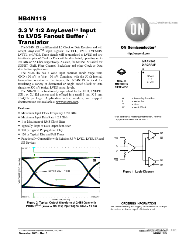
NB4N11S 3.3 V 1:2 AnyLevel™ Input to LVDS Fanout Buffer / Translator The NB4N11S is a differential 1:2 Clock or Data Receiver and will accept AnyLevel.
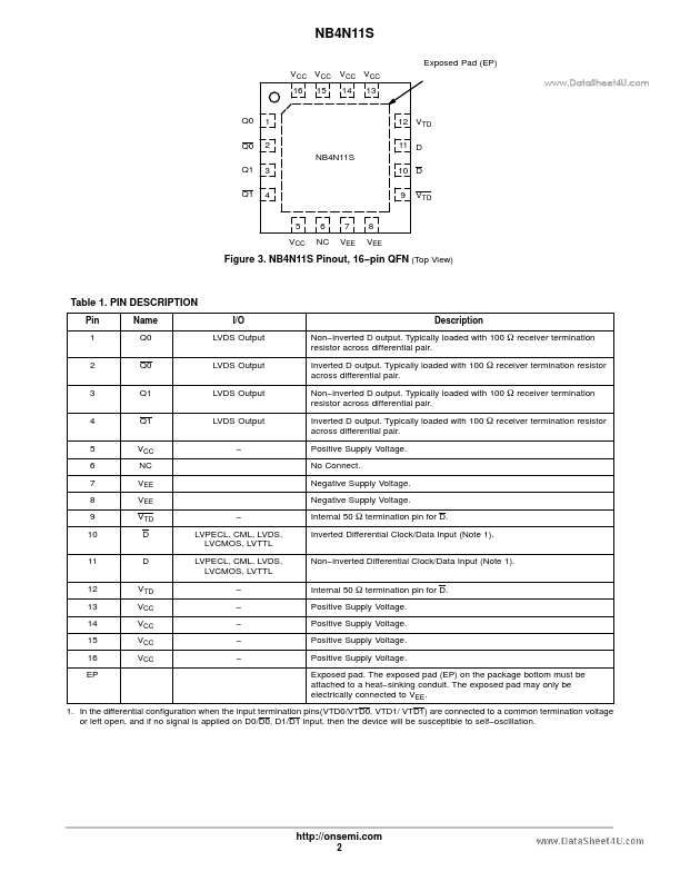
Pin 1 2 3 4 5 6 7 8 9 10 11 12 13 14 15 16 EP Name Q0 Q0 Q1 Q1 VCC NC VEE VEE VTD D D VTD VCC VCC VCC VCC.
LVPECL, CML, LVDS, LVCMOS, LVTTL L.
NB4N11S Features
* www. DataSheet4U. com
http://onsemi. com MARKING DIAGRAM
* 16 1
1 QFN
* 16 MN SUFFIX CASE 485G
NB4N 11S ALYW
A L Y W
= Assembly Location = Wafer Lot = Year = Work Week
* Maximum Input Clock Frequency > 2.0 GHz Maximum
NB4N11S Applications
* The NB4N11S has a wide input common mode range from GND + 50 mV to VCC
* 50 mV. Combined with the 50 W internal termination resistors at the inputs, the NB4N11S is ideal for translating a variety of differential or single
* ended Clock or Data signals to 350 mV typical LVDS output lev
📁 Related Datasheet
📌 All Tags