Datasheet Details
| Part number | NBSG53A |
|---|---|
| Manufacturer | ON Semiconductor ↗ |
| File Size | 162.14 KB |
| Description | 2.5V/3.3V SiGe Selectable Differential Clock and Data D Flip-Flop/Clock Divider |
| Datasheet |
 NBSG53A_ONSemiconductor.pdf NBSG53A_ONSemiconductor.pdf
|
| Part number | NBSG53A |
|---|---|
| Manufacturer | ON Semiconductor ↗ |
| File Size | 162.14 KB |
| Description | 2.5V/3.3V SiGe Selectable Differential Clock and Data D Flip-Flop/Clock Divider |
| Datasheet |
NBSG53A_ONSemiconductor.pdf
|
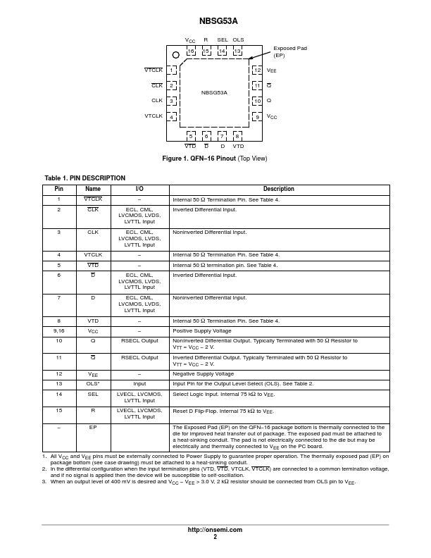
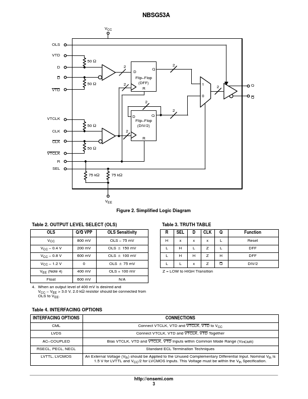
Pin Name I/O Description 1 VTCLK Internal 50 W Termination Pin. Internal 50 W Termination Pin. Internal 50 W termination pin.
📁 NBSG53A Similar Datasheet