Datasheet Details
| Part number | NBSG72A |
|---|---|
| Manufacturer | ON Semiconductor ↗ |
| File Size | 697.02 KB |
| Description | 2.5V/3.3V SiGe Differential 2 x 2 Crosspoint Switch |
| Datasheet |
 NBSG72A_ONSemiconductor.pdf NBSG72A_ONSemiconductor.pdf
|
| Part number | NBSG72A |
|---|---|
| Manufacturer | ON Semiconductor ↗ |
| File Size | 697.02 KB |
| Description | 2.5V/3.3V SiGe Differential 2 x 2 Crosspoint Switch |
| Datasheet |
NBSG72A_ONSemiconductor.pdf
|
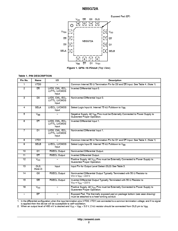
Pin No. LVDS, CML, ECL, LVTTL, LVCMOS Input LVDS, CML, ECL, LVTTL, LVCMOS Input LVECL, LVCMOS Input Inverted Differential Input 0.
📁 NBSG72A Similar Datasheet