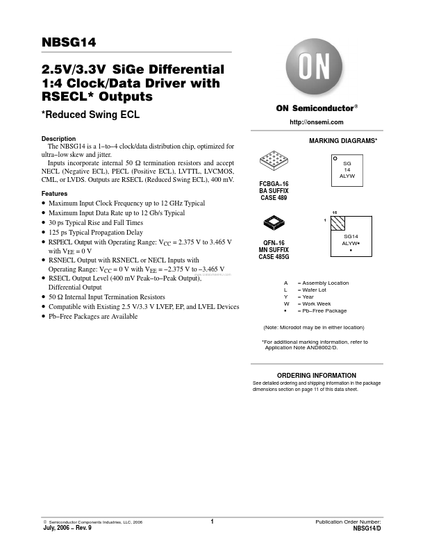
NBSG14
Overview
- Maximum Input Clock Frequency up to 12 GHz Typical Maximum Input Data Rate up to 12 Gb/s Typical 30 ps Typical Rise and Fall Times 125 ps Typical Propagation Delay RSPECL Output with Operating Range: VCC = 2.375 V to 3.465 V with VEE = 0 V RSNECL Output with RSNECL or NECL Inputs with Operating Range: VCC = 0 V with VEE = -2.375 V to -3.465 V RSECL Output Level (400 mV Peak-to-Peak Output), Differential Output 50 W Internal Input Termination Resistors Compatible with Existing 2.5 V/3.3 V LVEP, EP, and LVEL Devices Pb-Free Packages are Available