NBSG16
NBSG16 is SiGe Differential Receiver/Driver manufactured by onsemi.
Description
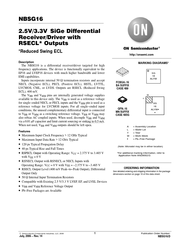
MARKING DIAGRAMS-
The NBSG16 is a differential receiver/driver targeted for high frequency applications. The device is functionally equivalent to the EP16 and LVEP16 devices with much higher bandwidth and lower EMI capabilities. Inputs incorporate internal 50 W termination resistors and accept NECL (Negative ECL), PECL (Positive ECL), HSTL, LVTTL, LVCMOS, CML, or LVDS. Outputs are RSECL (Reduced Swing ECL), 400 m V. The VBB and VMM pins are internally generated voltage supplies available to this device only. The VBB is used as a reference voltage for single- ended NECL or PECL inputs and the VMM pin is used as a reference voltage for LVCMOS inputs. For all single- ended input conditions, the unused plementary differential input is connected to VBB or VMM as a switching reference voltage. VBB or VMM may also rebias AC coupled inputs. When used, decouple VBB and VMM via a 0.01 m F capacitor and limit current sourcing or sinking to 0.5 m A. .. When not used, VBB and VMM outputs should be left open.
Features
SG 16 ALYW FCBGA- 16 BA SUFFIX CASE 489
QFN- 16 MN SUFFIX CASE 485G
ÇÇ ÇÇ
SG 16 ALYWG G
- -
- -
- -
- -
- -
- Maximum Input Clock Frequency > 12 GHz Typical Maximum Input Data Rate > 12 Gb/s Typical 120 ps Typical Propagation Delay 40 ps Typical Rise and Fall Times RSPECL Output with Operating Range: VCC = 2.375 V to 3.465 V with VEE = 0 V RSNECL Output with RSNECL or NECL Inputs with Operating Range: VCC = 0 V with VEE =
- 2.375 V to
- 3.465 V RSECL Output Level (400 m V Peak- to- Peak Output), Differential Output Only 50 W Internal Input Termination Resistors patible with Existing 2.5 V/3.3 V LVEP, EP, and LVEL Devices VBB and VMM Reference Voltage Output Pb- Free Packages are Available
A L Y W G
= Assembly Location = Wafer Lot = Year = Work Week = Pb- Free Package
(Note: Microdot may be in either location)
- For additional marking information, refer to Application Note AND8002/D.
ORDERING INFORMATION
See detailed ordering and shipping information...