NBSG14
NBSG14 is SiGe Differential 1:4 Clock/Data Driver manufactured by onsemi.
Description
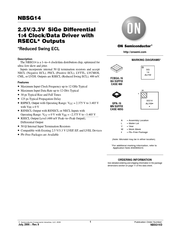
MARKING DIAGRAMS-
The NBSG14 is a 1- to- 4 clock/data distribution chip, optimized for ultra- low skew and jitter. Inputs incorporate internal 50 W termination resistors and accept NECL (Negative ECL), PECL (Positive ECL), LVTTL, LVCMOS, CML, or LVDS. Outputs are RSECL (Reduced Swing ECL), 400 m V.
Features
SG 14 ALYW FCBGA- 16 BA SUFFIX CASE 489
- -
- -
- -
- -
- -
Maximum Input Clock Frequency up to 12 GHz Typical Maximum Input Data Rate up to 12 Gb/s Typical 30 ps Typical Rise and Fall Times 125 ps Typical Propagation Delay RSPECL Output with Operating Range: VCC = 2.375 V to 3.465 V with VEE = 0 V RSNECL Output with RSNECL or NECL Inputs with Operating Range: VCC = 0 V with VEE =
- 2.375 V to
- 3.465 V .. RSECL Output Level (400 m V Peak- to- Peak Output), Differential Output 50 W Internal Input Termination Resistors patible with Existing 2.5 V/3.3 V LVEP, EP, and LVEL Devices Pb- Free Packages are Available
QFN- 16 MN SUFFIX CASE 485G
ÇÇÇ ÇÇÇ
16 1
SG14 ALYWG G
A L Y W G
= Assembly Location = Wafer Lot = Year = Work Week = Pb- Free Package
(Note: Microdot may be in either location)
- For additional marking information, refer to Application Note AND8002/D.
ORDERING INFORMATION
See detailed ordering and shipping information in the package dimensions section on page 11 of this data sheet.
© Semiconductor ponents Industries, LLC, 2006
July, 2006
- Rev. 9
Publication Order Number: NBSG14/D
1 A 2 3 4 VEE 16
VTCLK
Q0 15
Q0 14
VCC 13
Exposed Pad (EP)
Q3
Q3
Q2
VTCLK B
CLK VEE VCC Q2
1 2 NBSG14 3...