NBSG16VS
NBSG16VS is 2.5V/3.3V SiGe Differential Receiver/Driver manufactured by onsemi.
Description
The NBSG16VS is a differential receiver/driver targeted for high frequency applications that require variable output swing. The device is functionally equivalent to the EP16VS device with much higher bandwidth and lower EMI capabilities. This device may be used for applications driving VCSEL lasers. Inputs incorporate internal 50 W termination resistors and accept NECL (Negative ECL), PECL (Positive ECL), LVTTL, LVCMOS, CML, or LVDS. The output amplitude is varied by applying a voltage to the VCTRL input pin. Outputs are variable swing ECL from 100 m V to 750 m V amplitude, optimized for operation from VCC
- VEE = 3.0 V to 3.465 V. The VBB and VMM pins are internally generated voltage supplies available to this device only. The VBB is used as a reference voltage for single- ended NECL or PECL inputs and the VMM pin is used as a reference voltage for LVCMOS inputs. For single- ended input operation, the unused plementary differential input is connected to VBB or VMM as a switching reference voltage. VBB or VMM may also rebias AC coupled inputs. When used, decouple VBB and VMM via a .. 0.01 m F capacitor and limit current sourcing or sinking to 0.5 m A. When not used, VBB and VMM outputs should be left open.
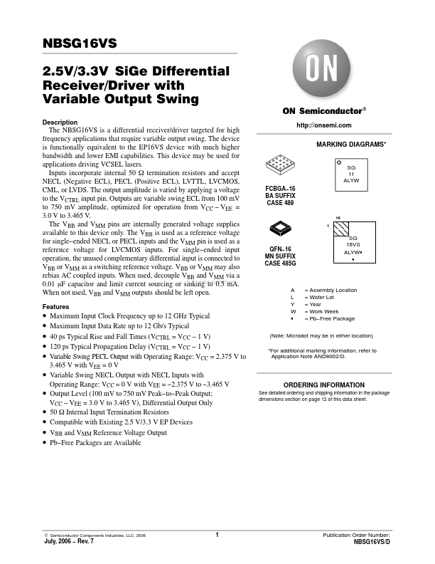
Features http://onsemi. MARKING DIAGRAMS-
SG 11 ALYW FCBGA- 16 BA SUFFIX CASE 489
QFN- 16 MN SUFFIX CASE 485G
ÇÇ ÇÇ
SG 16VS ALYWG G
- -
- -
- -
- -
- -
- Maximum Input Clock Frequency up to 12 GHz Typical Maximum Input Data Rate up to 12 Gb/s Typical 40 ps Typical Rise and Fall Times (VCTRL = VCC
- 1 V) 120 ps Typical Propagation Delay (VCTRL = VCC
- 1 V) Variable Swing PECL Output with Operating Range: VCC = 2.375 V to 3.465 V with VEE = 0 V Variable Swing NECL Output with NECL Inputs with Operating Range: VCC = 0 V with VEE =
- 2.375 V to
- 3.465 V Output Level (100 m V to 750 m V Peak- to- Peak Output; VCC
- VEE = 3.0 V to 3.465 V), Differential Output Only 50 W Internal Input Termination Resistors patible with Existing 2.5 V/3.3 V EP Devices VBB...