Datasheet Details
| Part number | NCD5701A |
|---|---|
| Manufacturer | ON Semiconductor |
| File Size | 338.23 KB |
| Description | High Current IGBT Gate Drivers |
| Datasheet |
 NCD5701A Datasheet NCD5701A Datasheet
|
|
|
| Part number | NCD5701A |
|---|---|
| Manufacturer | ON Semiconductor |
| File Size | 338.23 KB |
| Description | High Current IGBT Gate Drivers |
| Datasheet |
NCD5701A Datasheet
|
|
|
|
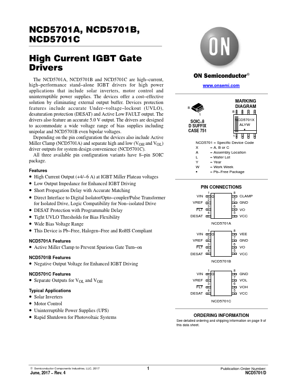
Pin Name No.I/O/x Description VIN 1 I Input signal to control the output.In applications which require galvanic isolation, VIN is generated at the opto output, the pulse transformer secondary or the digital isolator output.There is a signal inversion from VIN to VO (VOH/VOL).VIN is internally clamped to 5.5 V and has a pull up resistor of 1 MW to ensure that an output is low in the absence of an input signal. width is required at VIN before VO (VOH/VOL) i
📁 Similar Datasheet