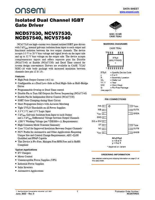
Description
Pin
Name
No.I/O
Description
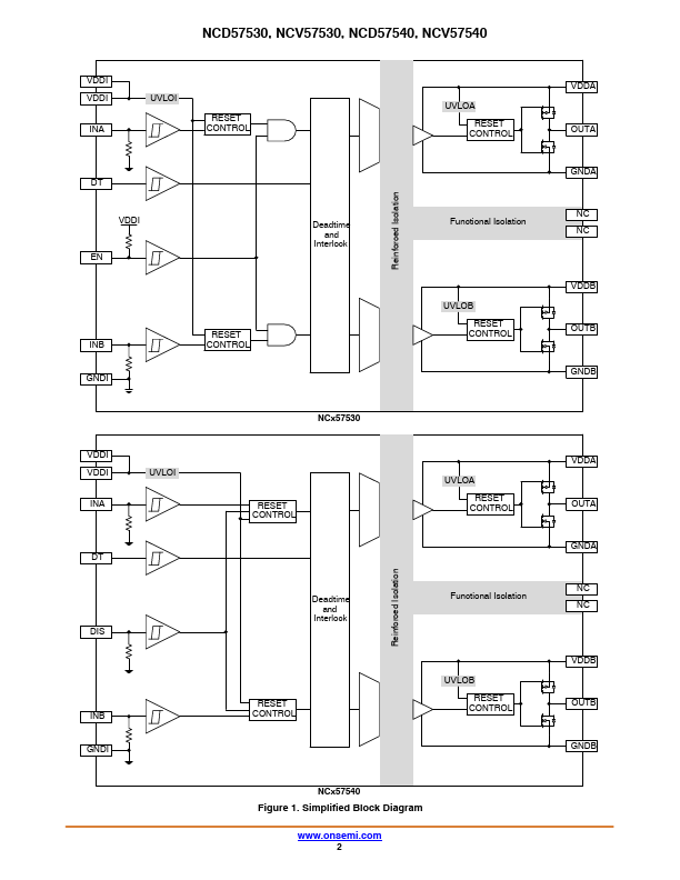
INA INB VDDI
1
Input A non-inverting gate driver input that defines OUTA.It has an equivalent pull
down resistor of 125 kW to
ensure that output is low in the absence of an input signal.A positive or negative going pulse with pulse width longer than maximum value of tMIN2 is required at INA before OUTA reacts.The input logic levels scale with VDDI up to VDDI = 5 V.With VDDI above 5 V the input logic levels stay the same as for VDDI = 5 V.Maxim
Features
- High Peak Output Current (±6.5 A).
- Configurable as a Dual Low.
- Side or Dual High.
- Side or Half.
- Bridge
Driver.
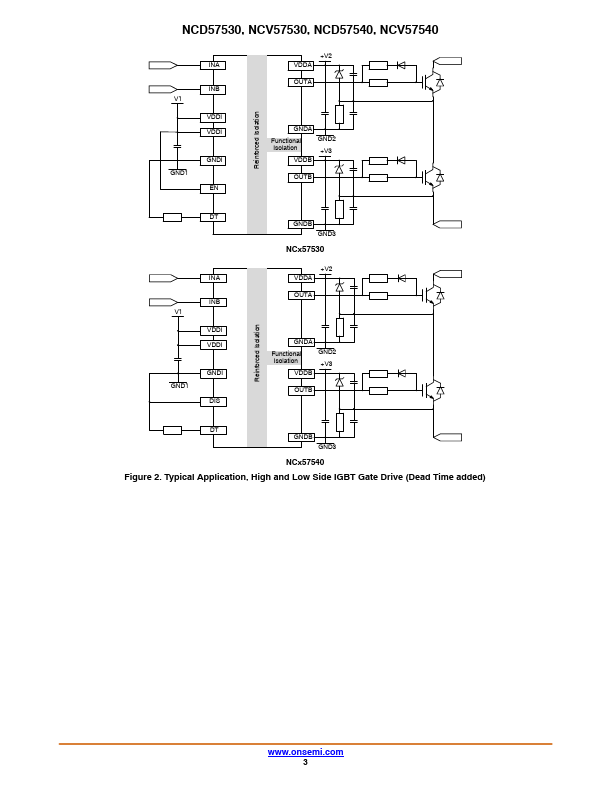
- Programmable Overlap or Dead Time control.
- Disable Pin to Turn Off Outputs for Power Sequencing (NCx57540).
- Enable Pin for Independent Driver Control (NCx57530).
- IGBT Gate Clamping during Short Circuit.
- Short Propagation Delays with Accurate Matching.
- Tight UVLO Thresholds on all Power Supplies.
 NCD57530-ONSemiconductor.pdf