Datasheet Details
| Part number | NCP1595 |
|---|---|
| Manufacturer | ON Semiconductor |
| File Size | 560.76 KB |
| Description | Current Mode PWM Converter |
| Datasheet |
 NCP1595 Datasheet NCP1595 Datasheet
|
|
|
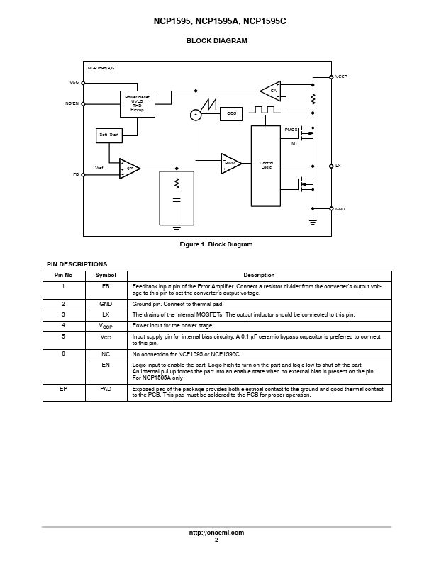
Figure 1.
Description Feedback input pin of the Error Amplifier.
Connect a resistor divider from the converter’s output voltage to this pin to set the converter’s output voltage.
| Part number | NCP1595 |
|---|---|
| Manufacturer | ON Semiconductor |
| File Size | 560.76 KB |
| Description | Current Mode PWM Converter |
| Datasheet |
NCP1595 Datasheet
|
|
|
|