Datasheet4U Logo Datasheet4U.com

NCP51190 - 1.5A DDR Memory Termination Regulator

Description

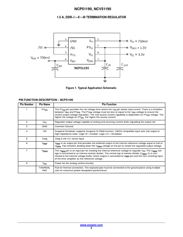
The PVCC pin provides the rail voltage from where the VTT pin draws load current.

between VCC and PVCC.

correct output voltage regulation.

Features

  • include extremely low initial offset voltage, excellent load regulation, source/sink soft.
  • start and on.
  • chip thermal shut.
  • down protection. The NCP/NCV51190 features the power.
  • saving Suspend To Ram (STR) function which will tri.
  • state the regulator output and lower the quiescent current drawn when the /SS pin is pulled low. The NCP/NCV51190 is available in a DFN8 package. Features.
  • Generate DDR Memory Termination Voltage (VTT).
  • For DDR.

📥 Download Datasheet

Datasheet preview – NCP51190

Datasheet Details

Part number NCP51190
Manufacturer onsemi
File Size 97.99 KB
Description 1.5A DDR Memory Termination Regulator
Datasheet download datasheet NCP51190 Datasheet
Additional preview pages of the NCP51190 datasheet.
Other Datasheets by ON Semiconductor

Full PDF Text Transcription

Click to expand full text
NCP51190, NCV51190 1.5A DDR Memory Termination Regulator The NCP/NCV51190 is a simple, cost−effective, high−speed linear regulator designed to generate the VTT termination voltage rail for DDR−I, DDR−II and DDR−III memory. The regulator is capable of actively sourcing or sinking up to ±1.5 A for DDR−I, or up to ±0.5 A for DDR−II /−III while regulating the output voltage to within ±30 mV. The output termination voltage is tightly regulated to track VTT = (VDDQ / 2) over the entire current range. The NCP/NCV51190 incorporates a high−speed differential amplifier to provide ultra−fast response to line and load transients. Other features include extremely low initial offset voltage, excellent load regulation, source/sink soft−start and on−chip thermal shut−down protection.
Published: |