Datasheet4U Logo Datasheet4U.com

NCP51401 Datasheet - ON Semiconductor

NCP51401 Termination Regulator

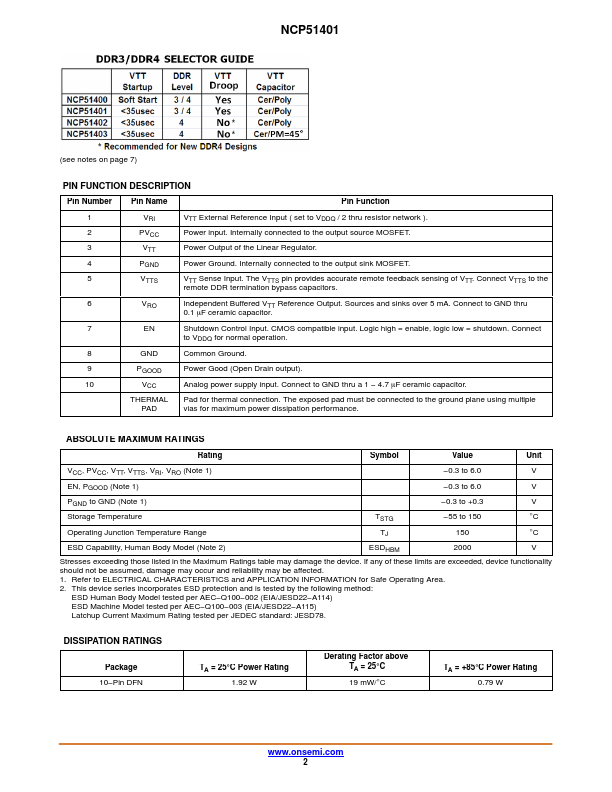
Pin Number Pin Name Pin Function 1 VRI VTT External Reference Input ( set to VDDQ / 2 thru resistor network ). 2 PVCC Power input. Internally connected to the output source MOSFET. 3 VTT Power Output of the Linear Regulator. 4 PGND Power Ground. Internally connected to the output sink .
3 Amp VTT Termination Regulator DDR1, DDR2, DDR3, LPDDR3, DDR4 NCP51401 The NCP51401 is a source/sink Double Data Rate (DDR) termination regulator specifically designed for low input voltage and low noise systems where space is a key consideration. The NCP51401 maintains a fast transient response and only requires a minimum output capacitance of 20 mF. The NCP51401 supports a remote sensing function and all power requirements for DDR VTT bus termination. The NCP51401 can also be used in .

NCP51401 Features

* Input Voltage Rails: Supports 2.5 V, 3.3 V and 5 V Rails

* PVCC Voltage Range: 1.1 to 3.5 V

* Integrated Power MOSFETs

* Source and Sink Termination Regulator with Droop Compensation

* Fast Load

* Transient Response

* PGOOD

* Logic outp

NCP51401 Datasheet (409.43 KB)

Preview of NCP51401 PDF
NCP51401 Datasheet Preview Page 2 NCP51401 Datasheet Preview Page 3

Datasheet Details

Part number:

NCP51401

Manufacturer:

ON Semiconductor ↗

File Size:

409.43 KB

Description:

Termination regulator.

📁 Related Datasheet

NCP51400 3Amp Termination Regulator (ON Semiconductor)

NCP51402 Termination Regulator (ON Semiconductor)

NCP51403 Termination Regulator (ON Semiconductor)

NCP51460 Micropower Precision Voltage Reference (ON Semiconductor)

NCP5104 Half Bridge Driver (ON Semiconductor)

NCP5106A High and Low Side Driver (ON Semiconductor)

NCP5106B High and Low Side Driver (ON Semiconductor)

NCP5109A High and Low Side Driver (ON Semiconductor)

TAGS

NCP51401 Termination Regulator ON Semiconductor

NCP51401 Distributor