Datasheet Details
| Part number | SN74LS174 |
|---|---|
| Manufacturer | ON Semiconductor |
| File Size | 178.06 KB |
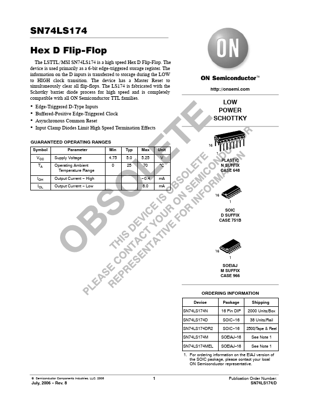
| Description | Hex D Flip-Flop |
| Datasheet |
 SN74LS174_ONSemiconductor.pdf SN74LS174_ONSemiconductor.pdf
|

| Part number | SN74LS174 |
|---|---|
| Manufacturer | ON Semiconductor |
| File Size | 178.06 KB |
| Description | Hex D Flip-Flop |
| Datasheet |
SN74LS174_ONSemiconductor.pdf
|
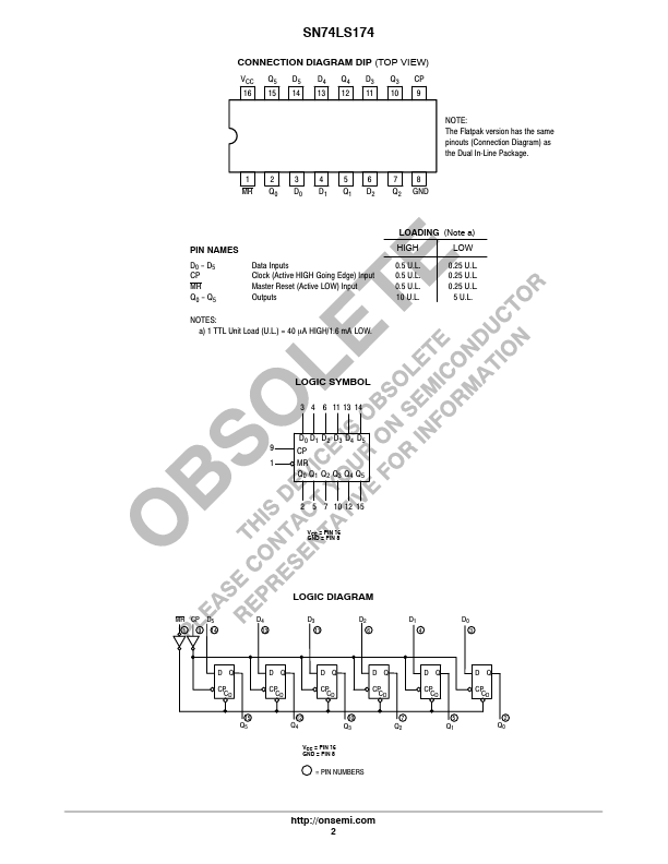
The LS174 consists of six edge-triggered D flip-flops with individual D inputs and Q outputs.
📁 SN74LS174 Similar Datasheet