Datasheet Details
- Part number
- NB4N527S
- Manufacturer
- ON Semiconductor ↗
- File Size
- 175.99 KB
- Datasheet
- NB4N527S_ONSemiconductor.pdf
- Description
- Dual AnyLevel to LVDS Receiver/Driver/Buffer/Translator
NB4N527S Description
NB4N527S 3.3V, 2.5Gb/s Dual AnyLevel™ to LVDS Receiver/Driver/Buffer/ Translator with Internal Input Termination NB4N527S is a clock or data Receiver.NB4N527S Applications
* as well as high speed logic interface where jitter and package size are main requirements. Application notes, models, and support documentation are available on www. onsemi. com.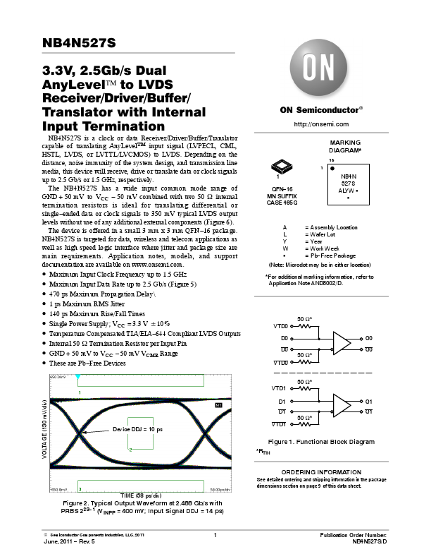
📁 Related Datasheet
📌 All Tags