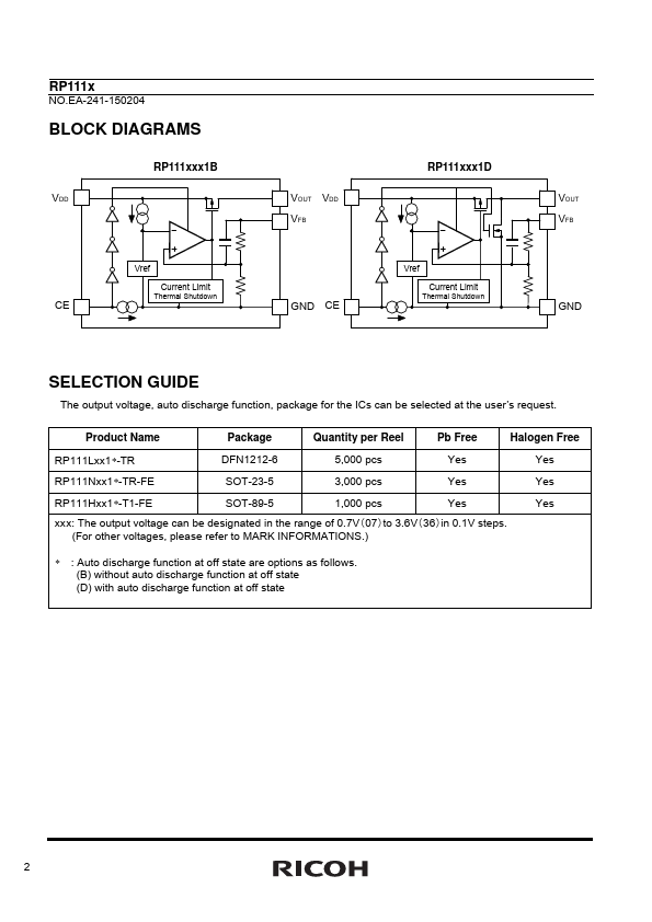
Description
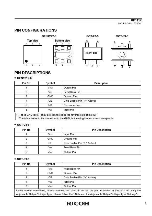
DFN1212-6
Pin No.Symbol
Description
1
VOUT
Output Pin
2 VFB Feed Back Pin
3
GND
Ground Pin
4 CE Chip Enable Pin ("H" Active)
5 NC No connection
6 VDD Input Pin
) Tab is GND level.(They are connected to the reverse side of this IC.) The tab is better to be connected to the GND, but leaving it open is also acceptable.
SOT-23-5
Pin No 1 2 3 4 5
Symbol VDD GND CE VFB VOUT
Pin Description Input Pin Ground Pin Chip Enable Pin ("H" Active) Feed Back Pin Output Pin
Features
- an excellent line transient response, ripple rejection at 75dB, and low noise. The output voltage accuracy is as high as ±0.8% and the temperature drift coefficient of output voltage is low at ±30ppm/C. The accuracy of the output voltage of RP111x includes the temperature characteristics and the load transient response has been improved. The typ. and max value of under/overshoot for various output current are shown in the typical characteristics in the datasheet, therefore the accuracy of the o.
 RP111x-RICOHelectronics.pdf