Datasheet4U Logo Datasheet4U.com

RD74LVC16374B Datasheet - Renesas Technology

16-bit D-type Flip Flops

RD74LVC16374B Features

* VCC = 1.65 V to 5.5 V All inputs VIH (Max.) = 5.5 V (@VCC = 0 V to 5.5 V) All outputs VOUT (Max.) = 5.5 V (@VCC = 0 V or output off state) Typical VOL ground bounce < 0.8 V (@VCC = 3.3 V, Ta = 25°C) Typical VOH undershoot > 2.0 V (@VCC = 3.

RD74LVC16374B General Description

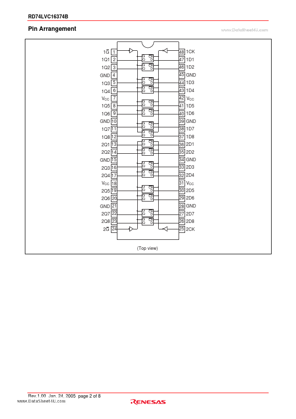
The RD74LVC16374B has sixteen edge trigger D type flip flops with three state outputs in a 48 pin package. Data at the D inputs meeting set up requirements are transferred to the Q outputs on positive going transitions of the clock input. When the latch enable goes low, data at the D inputs will be .

RD74LVC16374B Datasheet (105.75 KB)

Preview of RD74LVC16374B PDF

Datasheet Details

Part number:

RD74LVC16374B

Manufacturer:

Renesas ↗ Technology

File Size:

105.75 KB

Description:

16-bit d-type flip flops.

📁 Related Datasheet

RD74LVC16373B 16-bit D-type Transparent Latches (Renesas Technology)

RD74LVC16240B 16-bit Buffers / Line Drivers (Renesas Technology)

RD74LVC16244B 16-bit Buffers / Line Drivers (Renesas Technology)

RD74LVC16245B 16-bit Bus Transceivers (Renesas Technology)

RD74LVC125B Quad. Bus Buffer Gates (Renesas Technology)

RD74LVC126B Quad. Bus Buffer Gates (Renesas Technology)

RD74LVC138B 3-to-8-line Decoder / Demultiplexer (Renesas Technology)

RD74LVC139B Dual 2-to-4-line Decoders / Demultiplexers (Renesas Technology)

RD74LVC14B Hex Schmitt-trigger Inverters (Renesas Technology)

RD74LVC1G00 2-input NAND Gate (Renesas Technology)

TAGS

RD74LVC16374B 16-bit D-type Flip Flops Renesas Technology

Image Gallery

RD74LVC16374B Datasheet Preview Page 2 RD74LVC16374B Datasheet Preview Page 3

RD74LVC16374B Distributor