Datasheet Details
| Part number | HD74LV245A |
|---|---|
| Manufacturer | Renesas |
| File Size | 80.62 KB |
| Description | Octal Bus Transceivers |
| Datasheet |
 HD74LV245A Datasheet HD74LV245A Datasheet
|
|
|
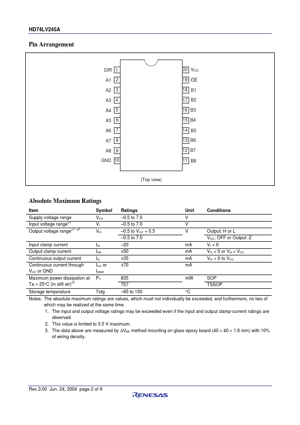
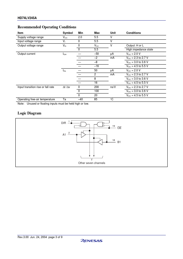
The HD74LV245A has eight buffers with three-state outputs in a 20-pin package.
When DIR is high, data is transferred from the A inputs to the B outputs, and when DIR is low, data is transferred from the B inputs to the A outputs.
| Part number | HD74LV245A |
|---|---|
| Manufacturer | Renesas |
| File Size | 80.62 KB |
| Description | Octal Bus Transceivers |
| Datasheet |
HD74LV245A Datasheet
|
|
|
|