Datasheet4U Logo Datasheet4U.com

IDT5V2310 Datasheet - Renesas

HIGH PERFORMANCE CLOCK BUFFER

IDT5V2310 Features

* High performance 1:10 clock driver for general purpose applications

* Operates up to 200MHz at VDD = 3.3V

* Pin-to-pin skew < 100ps

* VDD range: 2.3V to 3.6V

* Output enable glitch suppression

* Distributes one clock input to two banks of five outpu

IDT5V2310 General Description

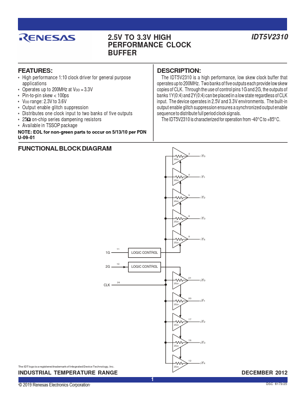
The IDT5V2310 is a high performance, low skew clock buffer that operates up to 200MHz. Two banks of five outputs each provide low skew copies of CLK. Through the use of control pins 1G and 2G, the outputs of banks 1Y(0:4) and 2Y(0:4) can be placed in a low state regardless of CLK input. The device .

IDT5V2310 Datasheet (214.41 KB)

Preview of IDT5V2310 PDF

Datasheet Details

Part number:

IDT5V2310

Manufacturer:

Renesas ↗

File Size:

214.41 KB

Description:

High performance clock buffer.

📁 Related Datasheet

IDT5V2310 2.5V TO 3.3V HIGH PERFORMANCE CLOCK BUFFER (Integrated Device Technology)

IDT5V2305 2.5V TO 3.3V HIGH PERFORMANCE CLOCK BUFFER (Integrated Device)

IDT5V2305 HIGH PERFORMANCE CLOCK BUFFER (Renesas)

IDT5V2528 2.5V / 3.3V PHASE-LOCK LOOP CLOCK DRIVER ZERO DELAY BUFFER (Integrated Device)

IDT5V2528A 2.5V / 3.3V PHASE-LOCK LOOP CLOCK DRIVER ZERO DELAY BUFFER (Integrated Device)

IDT5V19EE604 EEPROM PROGRAMMABLE VCXO CLOCK GENERATOR (Renesas)

IDT5V40501 PLL CLOCK MULTIPLIER (IDT)

IDT5V40501 PLL CLOCK MULTIPLIER (Renesas)

IDT5V41065 2 OUTPUT PCIE GEN1/2 SYNTHESIZER (IDT)

IDT5V41066 4 OUTPUT PCIE GEN1/2 SYNTHESIZER (IDT)

TAGS

IDT5V2310 HIGH PERFORMANCE CLOCK BUFFER Renesas

Image Gallery

IDT5V2310 Datasheet Preview Page 2 IDT5V2310 Datasheet Preview Page 3

IDT5V2310 Distributor