Datasheet Details
| Part number | MB84VD21181EM-70 |
|---|---|
| Manufacturer | SPANSION |
| File Size | 895.73 KB |
| Description | (MB84VD2118xEM-70 / MB84VD2119xEM-70) Stacked MCP (Multi-Chip Package) FLASH MEMORY |
| Datasheet |
 MB84VD21181EM-70_SPANSION.pdf MB84VD21181EM-70_SPANSION.pdf
|
| Part number | MB84VD21181EM-70 |
|---|---|
| Manufacturer | SPANSION |
| File Size | 895.73 KB |
| Description | (MB84VD2118xEM-70 / MB84VD2119xEM-70) Stacked MCP (Multi-Chip Package) FLASH MEMORY |
| Datasheet |
MB84VD21181EM-70_SPANSION.pdf
|
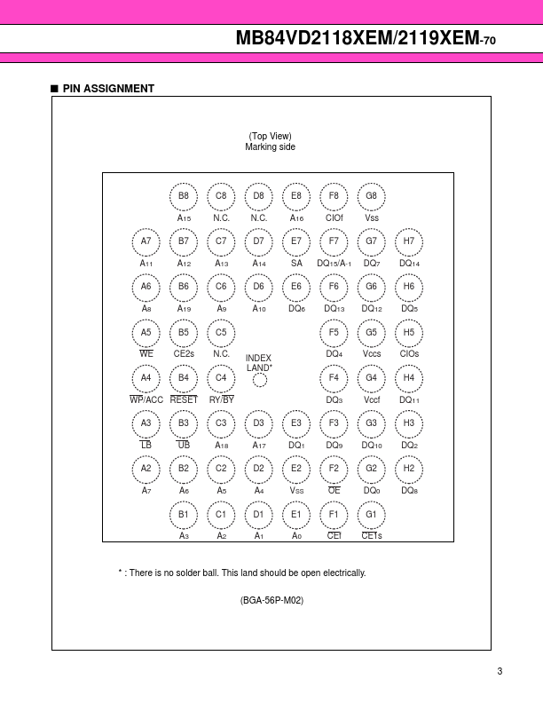
Pin Name A17 to A0 A19, A18, A-1 SA DQ15 to DQ0 CEf CE1s CE2s OE WE RY/BY UB LB CIOf Function Address Inputs (Common) Address Input (Flash) Address Input (SRAM) Data Inputs / Outputs (Common) Chip Enable (Flash) Chip Enable (SRAM) Chip Enable (SRAM) Output Enable (Common) Write Enable (Common) Ready/Busy Outputs (Flash) Open Drain Output Upper Byte Control (SRAM) Lower Byte Control (SRAM) I/O Configuration (Flash) CIOf=VCCf is Word mode ( ×16), CIOf=VSS is Byte mode ( × 8) I/O Configuration (SRA
📁 MB84VD21181EM-70 Similar Datasheet