Datasheet Details
| Part number | MB84VD21191EM-70, MB84VD21181EM-70 |
|---|---|
| Manufacturer | SPANSION |
| File Size | 895.73 KB |
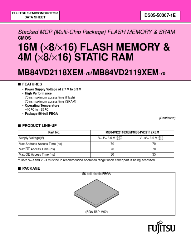
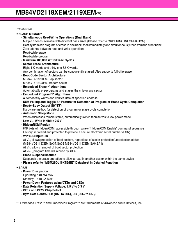
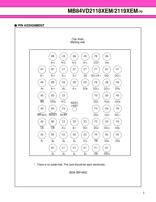
| Description | (MB84VD2118xEM-70 / MB84VD2119xEM-70) Stacked MCP (Multi-Chip Package) FLASH MEMORY |
| Datasheet |
|
| Note |
This datasheet PDF includes multiple part numbers: MB84VD21191EM-70, MB84VD21181EM-70. Please refer to the document for exact specifications by model. |


