Datasheet Details
| Part number | STP40N20 |
|---|---|
| Manufacturer | STMicroelectronics |
| File Size | 388.33 KB |
| Description | N-CHANNEL MOSFET |
| Datasheet |
 STP40N20 Datasheet STP40N20 Datasheet
|
|
|
| Part number | STP40N20 |
|---|---|
| Manufacturer | STMicroelectronics |
| File Size | 388.33 KB |
| Description | N-CHANNEL MOSFET |
| Datasheet |
STP40N20 Datasheet
|
|
|
|
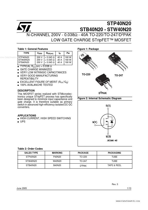
This MOSFET series realized with STMicroelectronics unique STripFET process has specifically been designed to minimize input capacitance and gate charge. HIGH CURRENT, HIGH SPEED SWITCHING UPS Table 2: Order Codes SALES TYPE STP40N20 STW40N20 STB40N20 MARKING P40N20 W40N20 B40N20 PACKAGE TO-220 TO-247 D2PAK PACKAGING TUBE TUBE
📁 Similar Datasheet