Description
2.3 Addressing
3. Absolute Maximum Rating
4. AC & DC Operating Conditions & Specifications
Page 2 of 28
Rev.1.1 Aug.2005
1G A-die DDR2 SDRAM
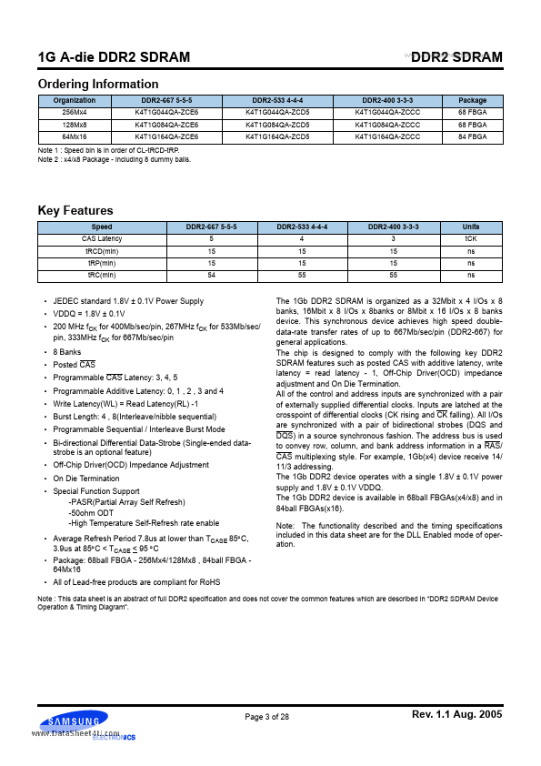
Ordering Information
Organization 256Mx4 128Mx8 64Mx16 DDR2-667 5-5-5 K4T1G044QA-ZCE6 K4T1G084QA-ZCE6 K4T1G164QA-ZCE6 DDR2-533 4-4-4 K4T1G044QA-ZCD5 K4T1G084QA-ZCD5 K4T1G164QA-ZCD5
www.DataSheet4U.com
DDR2 SDRAM
Package 68 FBGA 68 FBGA 84 FBGA
DDR2-400 3-3-3 K4T1G044QA-ZCCC K4T1G084QA-ZCCC K4T1G164QA-ZCCC
Note 1 : Speed bin is in order of CL-tRCD
Features
- Speed CAS Latency tRCD(min) tRP(min) tRC(min) DDR2-667 5-5-5 5 15 15 54 DDR2-533 4-4-4 4 15 15 55 DDR2-400 3-3-3 3 15 15 55 Units tCK ns ns ns.
- JEDEC standard 1.8V ± 0.1V Power Supply.
- VDDQ = 1.8V ± 0.1V.
- 200 MHz fCK for 400Mb/sec/pin, 267MHz fCK for 533Mb/sec/ pin, 333MHz fCK for 667Mb/sec/pin.
- 8 Banks.
- Posted CAS.
- Programmable CAS Latency: 3, 4, 5.
- Programmable Additive Latency: 0, 1 , 2 , 3 and 4.
- Write Latency(WL) = Rea.
 K4T1G164QA_Samsungsemiconductor.pdf