Datasheet Details
- Part number
- K7J161882B
- Manufacturer
- Samsung semiconductor
- File Size
- 418.32 KB
- Datasheet
- K7J161882B_Samsungsemiconductor.pdf
- Description
- (K7J161882B / K7J163682B) 512Kx36 & 1Mx18 DDR II SIO b2 SRAM
K7J161882B Description
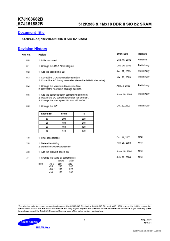
K7J163682B K7J161882B www.DataSheet4U.com Document Title 512Kx36 & 1Mx18 DDR II SIO b2 SRAM 512Kx36-bit, 1Mx18-bit DDR II SIO b2 SRAM Revision Hist.
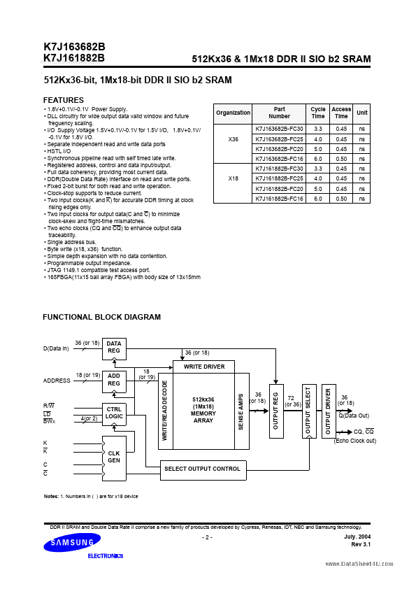
Input Clock Input Clock for Output Data Output Echo Clock DLL Disable when low Address Inputs Data Inputs 1 NOTE
Q0-35
Data Outputs Read, Write Cont.
K7J161882B Features
* 1.8V+0.1V/-0.1V Power Supply.
* DLL circuitry for wide output data valid window and future freguency scaling.
* I/O Supply Voltage 1.5V+0.1V/-0.1V for 1.5V I/O, 1.8V+0.1V/ -0.1V for 1.8V I/O.
* Separate independent read and write data ports
* HSTL I/O

📁 Related Datasheet
📌 All Tags