Datasheet4U Logo Datasheet4U.com

K7J163682B, K7J161882B Datasheet - Samsung semiconductor

K7J161882B_Samsungsemiconductor.pdf

This datasheet PDF includes multiple part numbers: K7J163682B, K7J161882B. Please refer to the document for exact specifications by model.
K7J163682B Datasheet Preview Page 2 K7J163682B Datasheet Preview Page 3

Datasheet Details

Part number:

K7J163682B, K7J161882B

Manufacturer:

Samsung semiconductor

File Size:

418.32 KB

Description:

(k7j161882b / k7j163682b) 512kx36 & 1mx18 ddr ii sio b2 sram.

Note:

This datasheet PDF includes multiple part numbers: K7J163682B, K7J161882B.
Please refer to the document for exact specifications by model.

K7J163682B, K7J161882B, (K7J161882B / K7J163682B) 512Kx36 & 1Mx18 DDR II SIO b2 SRAM

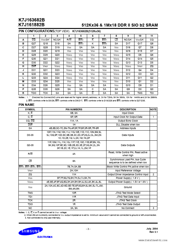
Input Clock Input Clock for Output Data Output Echo Clock DLL Disable when low Address Inputs Data Inputs 1 NOTE Q0-35 Data Outputs Read, Write Control Pin, Read active when high Synchronous Load Pin, bus Cycle sequence is to be defined when low Block Write Control Pin,active when low Input Refere

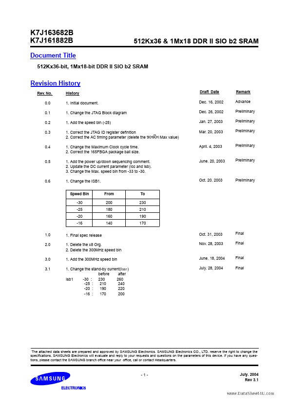
K7J163682B K7J161882B www.DataSheet4U.com Document Title 512Kx36 & 1Mx18 DDR II SIO b2 SRAM 512Kx36-bit, 1Mx18-bit DDR II SIO b2 SRAM Revision History Rev.

No.

0.0 0.1 0.2 0.3 History 1.

Initial document.

1.

Change the JTAG Block diagram 1.

Add the speed bin (-25) 1.

Correct the JTAG ID register definition 2.

Correct the AC timing parameter (delete the tKHKH Max value) 1.

Change the Maximum Clock cycle time.

2.

Correct the 165FBGA package ball size.

1.

Add the power up/down sequencing comment

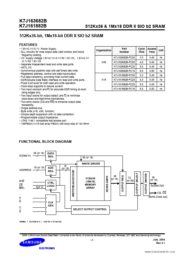
K7J163682B Features

* 1.8V+0.1V/-0.1V Power Supply.

* DLL circuitry for wide output data valid window and future freguency scaling.

* I/O Supply Voltage 1.5V+0.1V/-0.1V for 1.5V I/O, 1.8V+0.1V/ -0.1V for 1.8V I/O.

* Separate independent read and write data ports

* HSTL I/O

📁 Related Datasheet

📌 All Tags

Samsung semiconductor K7J163682B-like datasheet