Description
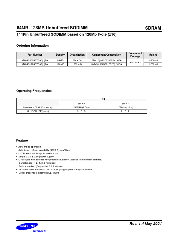
Pin Name A0 ~ A11 BA0 ~ BA1 DQ0 ~ DQ63 CLK0 ~ CLK1 CKE0 ~ CKE1 CS0 ~ CS1 RAS CAS Select bank Data input/output Clock input Clock enable input Chip select input Row address strobe Column address strobe Function Address input (Multiplexed) WE DQM0 ~ 7 VDD VSS SDA SCL DU NC Pin Name Write enable DQM Power supply (3.3V) Ground Serial data I/O Serial clock Don′t use No connection Function
SA
Features
- ess otherwise noted, TA = 0 to 70°C) Version Parameter Symbol Test Condition 7A Operating current (One b.
 M464S0924FTS_Samsungsemiconductor.pdf