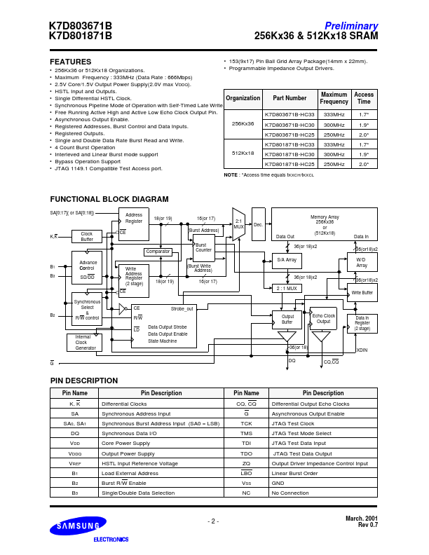
Description
Pin Name K, K SA
SA0, SA1 DQ VDD VDDQ VREF B1 B2 B3
Pin Description Differential Clocks Synchronous Address Input Synchronous Burst Address Input (SA0 = LSB) Synchronous Data I/O Core Power Supply Output Power Supply HSTL Input Reference Voltage Load External Address Burst R/W Enable Single/Double Data Selection
2:1 MUX
Dec.Data Out
Memory Array 256Kx36 or (512Kx18)
36(or 18)x2
S/A Array
36(or 18)x2 2 : 1 MUX
Data In 36(or18)x2 W/D Array
36(or18)x2
Write Buffer
Output Buffer
Echo Cl
Features
- 256Kx36 or 512Kx18 Organizations.
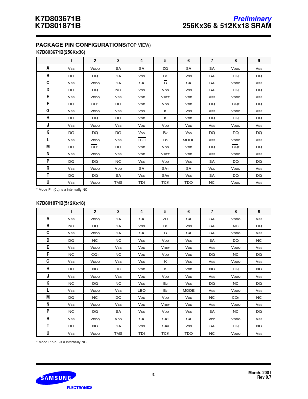
- 153(9x17) Pin Ball Grid Array Package(14mm x 22mm).
- Programmable Impedance Output Drivers.
- Maximum Frequency : 333MHz (Data Rate : 666Mbps).
- 2.5V Core/1.5V Output Power Supply(2.0V max VDDQ).
- HSTL Input and Outputs.
- Single Differential HSTL Clock. Organization.
- Synchronous Pipeline Mode of Operation with Self-Timed Late Write. Part Number
Maximum Access Frequency Time.
 K7D803671B-Samsung.pdf