Datasheet Details
| Part number | K7D803671B |
|---|---|
| Manufacturer | Samsung |
| File Size | 299.69 KB |
| Description | SRAM |
| Datasheet |
 K7D803671B-Samsung.pdf K7D803671B-Samsung.pdf
|
| Part number | K7D803671B |
|---|---|
| Manufacturer | Samsung |
| File Size | 299.69 KB |
| Description | SRAM |
| Datasheet |
K7D803671B-Samsung.pdf
|
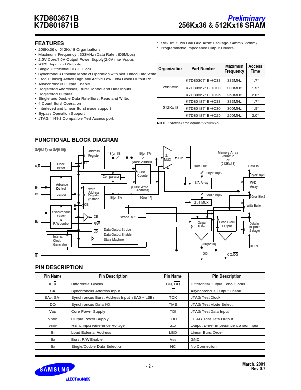
Pin Name K, K SA SA0, SA1 DQ VDD VDDQ VREF B1 B2 B3 Pin Description Differential Clocks Synchronous Address Input Synchronous Burst Address Input (SA0 = LSB) Synchronous Data I/O Core Power Supply Output Power Supply HSTL Input Reference Voltage Load External Address Burst R/W Enable Single/Double Data Selection 2:1 MUX Dec.Data Out Memory Array 256Kx36 or (512Kx18) 36(or 18)x2 S/A Array 36(or 18)x2 2 : 1 MUX Data In 36(or18)x2 W/D Array 36(or18)x2 Write Buffer Output Buffer Echo Cl
📁 K7D803671B Similar Datasheet