Datasheet Details
- Part number
- HYS64V2100GU-10
- Manufacturer
- Siemens
- File Size
- 75.48 KB
- Datasheet
- HYS64V2100GU-10_SiemensSemiconductorGroup.pdf
- Description
- 3.3V 2M x 64-Bit SDRAM Module 3.3V 2M x 72-Bit SDRAM Module
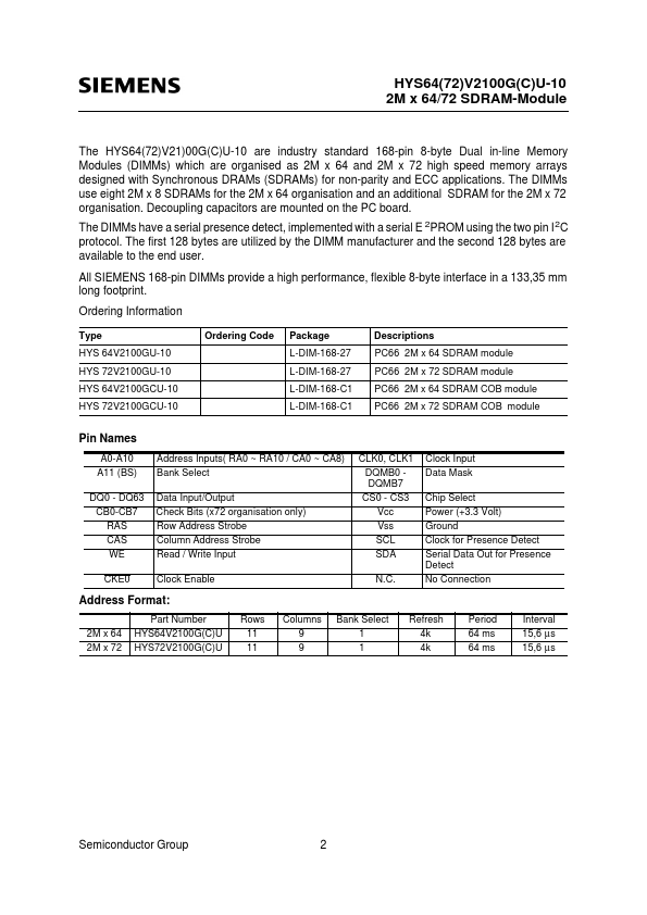
HYS64V2100GU-10 Description
3.3V 2M x 64-Bit SDRAM Module 3.3V 2M x 72-Bit SDRAM Module 168 pin unbuffered DIMM Modules HYS64V2100G(C)U-10 HYS72V2100G(C)U-10 * 168 Pin.HYS64V2100GU-10 Features
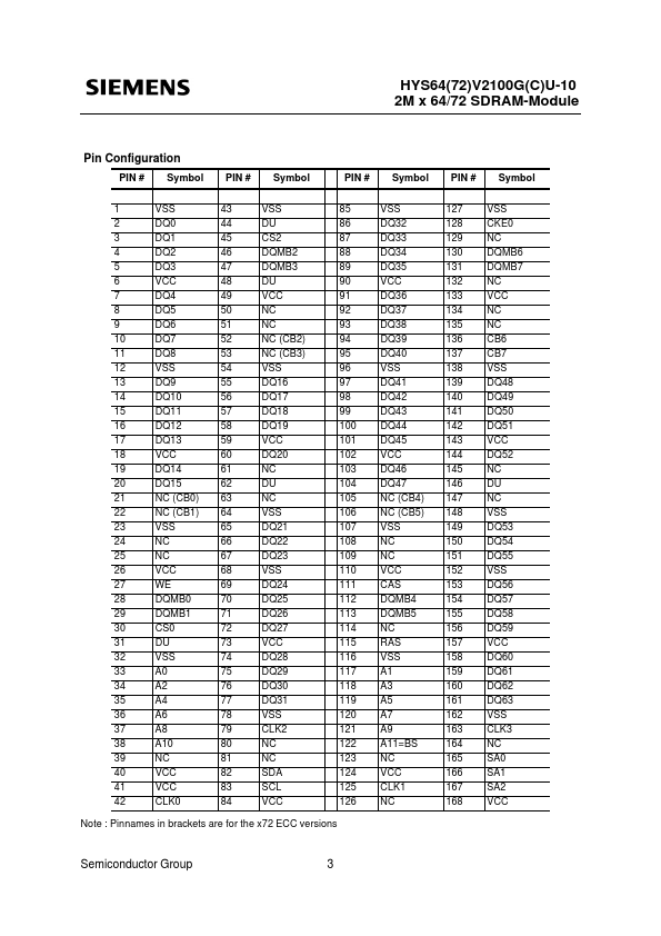
* d after power-up, then a Precharge All Banks command must be given followed by 8 Auto Refresh (CBR) cycles before the Mode Register Set Operation can begin. 4. AC timing tests have V il = 0.4 V and V ih = 2.4 V with the timing referenced to the 1.4 V crossover point. The transition time is measuredHYS64V2100GU-10 Applications
* 1 bank 2M x 64, 2M x 72 organisation Optimized for byte-write non-parity or ECC applications Fully PC66 layout compatible JEDEC standard Synchronous DRAMs (SDRAM) Performance: -10 fCK tAC Max. Clock frequency Max. access time from clock 66 MHz @ CL=2 100 MHz @ CL=3 9 ns @ CL=2 8 ns @ CL=3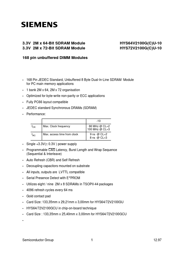
📁 Related Datasheet
📌 All Tags