Click to expand full text
TA2026SN / F
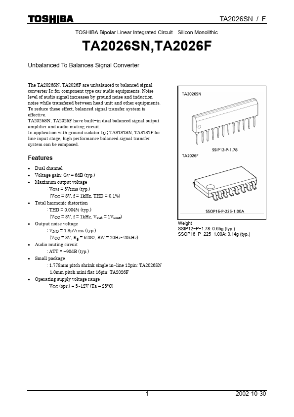
TOSHIBA Bipolar Linear Integrated Circuit Silicon Monolithic
TA2026SN,TA2026F
Unbalanced To Balances Signal Converter
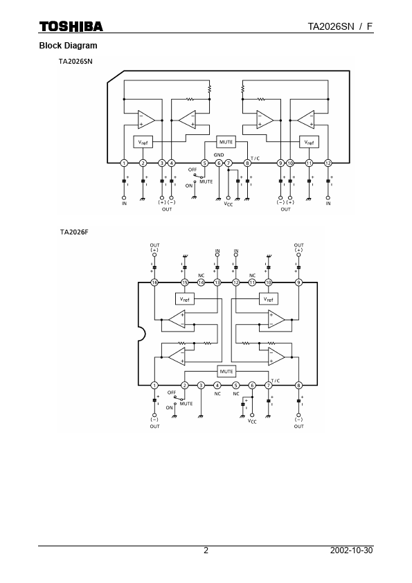
The TA2026SN, TA2026F are unbalanced to balanced signal converter IC for component type car audio equipments. Noise level of audio signal increases by ground noise and induction noise while transfered between head unit and other equipments. To reduce these effect, balanced signal transfer system is effective. TA2026SN, TA2026F have built−in dual balanced signal output amplifier and audio muting circuit. In application with ground isolator IC ; TA8181SN, TA8181F for line input stage, high performance balanced signal transfer system can be composed.
Features
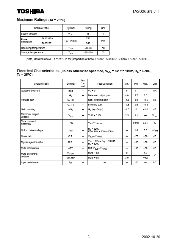
· Dual channel · Voltage gain: GV = 6dB (typ.) · Maximum output voltage
: VOM = 3Vrms (typ.
 TA2026SN Datasheet