Datasheet4U Logo Datasheet4U.com

GA1086 11-Output Clock Buffer

📥 Download Datasheet  Datasheet Preview Page 1

Description

T R I Q U I N T S E M I C O N D U C T O R, I N C .Figure 1.Block Diagram FBIN 11 GA1086 S1 10 CLK 9 S0 8 NC 7 NC 6 GND 5 S2 12 VDD.
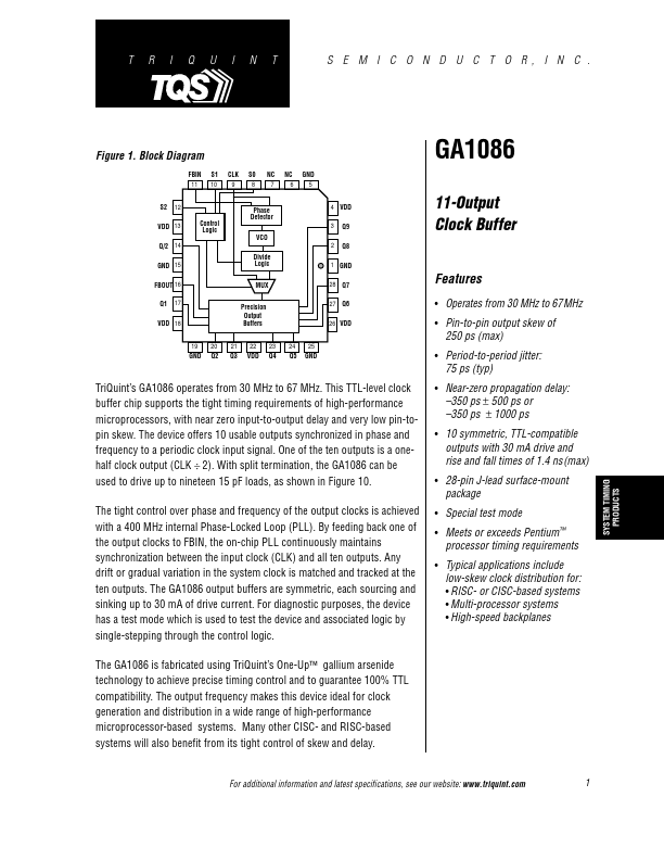
The GA1086 generates 10 outputs (Q1. Q9 and FBOUT) which have the same frequency and zero phase delay relative to the reference clock input.

📥 Download Datasheet

Preview of GA1086 PDF
datasheet Preview Page 2 datasheet Preview Page 3

Datasheet Specifications

Part number
GA1086
Manufacturer
TriQuint Semiconductor
File Size
234.88 KB
Datasheet
GA1086_TriQuintSemiconductor.pdf
Description
11-Output Clock Buffer

Features

* Operates from 30 MHz to 67MHz
* Pin-to-pin output skew of 250 ps (max)
* Period-to-period jitter: 75 ps (typ)
* Near-zero propagation delay:
* 350 ps ± 500 ps or
* 350 ps ± 1000 ps
* 10 symmetric, TTL-compatible outputs with 30 mA drive and ris

Applications

* include low-skew clock distribution for:
* RISC- or CISC-based systems
* Multi-processor systems

GA1086 Distributors

📁 Related Datasheet

📌 All Tags

TriQuint Semiconductor GA1086-like datasheet